My Cart
Your Cart 0

    Your cart is empty.

  • Total (Amount) ₹0.00
NCERT Exemplar · Class 12 · Physics

Chapter 14: Semiconductor Electronics: Materials, Devices and Simple Circuits

Practice each question, then open the answer or worked solution.

Questions

38 questions
Q14.1Written answer

The conductivity of a semiconductor increases with increase in temperature because

(a) number density of free current carriers increases

(b) relaxation time increases

(c) both number density of carriers and relaxation time increase

(d) number density of current carriers increases, relaxation time decreases but the effect of a decrease in relaxation time is much less than the increase in number density
Show solutionHide solution
Worked solution

(d) number density of current carriers increases, relaxation time decreases but the effect of a decrease in relaxation time is much less than the increase in number density
Q14.2Written answer

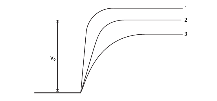
In the figure, Vo is the potential barrier across a p-n junction, when no battery is connected across the junction

Exemplar Solutions Class 12 Physics Chapter 14 - 1

(a) 1 and 3 both correspond to forward bias of junction

(b) 3 corresponds to forward bias of junction and 1 corresponds to reverse bias of junction

(c) 1 corresponds to forward bias and 3 corresponds to reverse bias of junction

(d) 3 and 1 both correspond to reverse bias of junction

Show solutionHide solution
Worked solution

(b) 3 corresponds to forward bias of junction and 1 corresponds to reverse bias of junction

Q14.3Written answer

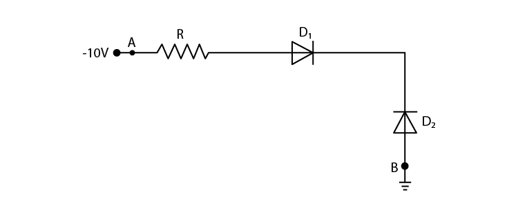
In the figure, assuming the diodes to be ideal,

Exemplar Solutions Class 12 Physics Chapter 14 - 2

(a) D1 is forward biased and D2 is reverse biased and hence current flows from A to B

(b) D2 is forward biased and D1 is reverse biased and hence no current flows from B to A and vice versa

(c) D1 and D2 are both forward biased and hence current flows from A to B

(d) D1 and D2 are both reverse biased and hence no current flows from A to B and vice versa

Show solutionHide solution
Worked solution

(b) D2 is forward biased and D1 is reverse biased and hence no current flows from B to A and vice versa

Q14.4Written answer

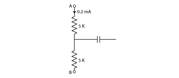
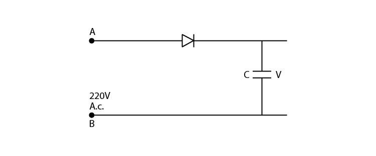
A 220 V A.C. supply is connected between points A and B in the figure. What will be the potential difference V across the capacitor?

Exemplar Solutions Class 12 Physics Chapter 14 - 3

(a) 220V

(b) 110V

(c) 0V

(d) 220 √2 V

Show solutionHide solution
Worked solution

(d) 220 √2 V

Q14.5Written answer

Hole is

(a) an anti-particle of the electron

(b) a vacancy created when an electron leaves a covalent bond

(c) absence of free electrons

(d) an artificially created particle

Show solutionHide solution
Worked solution

(b) a vacancy created when an electron leaves a covalent bond

Q14.6Written answer

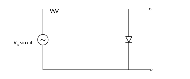
The output of the given circuit in the figure

Exemplar Solutions Class 12 Physics Chapter 14 - 4

(a) would be zero at all times

(b) would be like a half-wave rectifier with positive cycles in output

(c) would be like a half-wave rectifier with negative cycles in output

(d) would be like that of a full-wave rectifier

Show solutionHide solution
Worked solution

(c) would be like a half-wave rectifier with negative cycles in output

Q14.7Written answer

In the circuit shown in the figure, if the diode forward voltage drop is 0.3 V, the voltage difference between A and B is

Exemplar Solutions Class 12 Physics Chapter 14 - 5

(a) 1.3 V

(b) 2.3 V

(c) 0

(d) 0.5 V

Show solutionHide solution
Worked solution

(b) 2.3 V

Q14.8Written answer

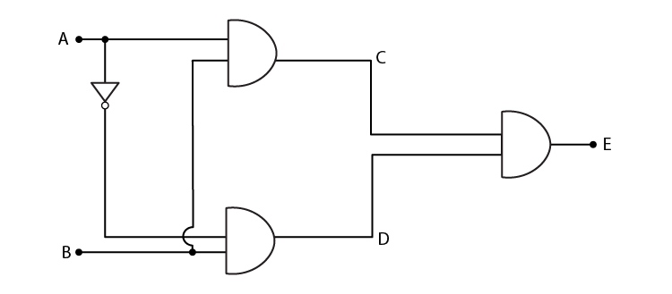
Truth table for the given circuit in the figure is

Exemplar Solutions Class 12 Physics Chapter 14 - 6

(a)

A B E
0 0 1
0 1 0
1 0 1
1 1 0

(b)

A B E
0 0 1
0 1 0
1 0 0
1 1 1

(c)

A B E
0 0 0
0 1 1
1 0 0
1 1 1

(d)

A B E
0 0 0
0 1 1
1 0 1
1 1 0
Show solutionHide solution
Worked solution

(c)

A B E
0 0 0
0 1 1
1 0 0
1 1 1
Multiple Choice Questions II
Q14.9Written answer

When an electric field is applied across a semiconductor

(a) electrons move from lower energy level to higher energy level in the conduction band

(b) electrons move from higher energy level to lower energy level in the conduction band

(c) holes in the valence band move from higher energy level to lower energy level

(d) holes in the valence band move from lower energy level to higher energy level

Show solutionHide solution
Worked solution

(a) electrons move from lower energy level to higher energy level in the conduction band

(c) holes in the valence band move from higher energy level to lower energy level

Q14.10Multiple choice

Consider an NPN transistor with its base-emitter junction forward biased and collector-base junction reverse biased. Which of the following statements are true?

Show answerHide answer
Correct option: A
Show solutionHide solution
Worked solution

(a) Electrons crossover from emitter to collector

(c) Electrons move from emitter to base