My Cart
Your Cart 0

    Your cart is empty.

  • Total (Amount) ₹0.00
NCERT Exemplar · Class 12 · Physics

Chapter 14: Semiconductor Electronics: Materials, Devices and Simple Circuits

Practice each question, then open the answer or worked solution.

Questions

38 questions
Q14.11Multiple choice

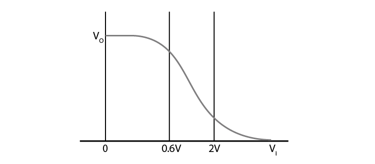
In the figure shows the transfer characteristics of a base biased CE transistor. Which of the following statements are true?
Exemplar Solutions Class 12 Physics Chapter 14 - 7

Show answerHide answer
Correct option: B
Show solutionHide solution
Worked solution

(b) At Vi = 1V, it can be used as an amplifier

(c) At Vi = 0. .5V, it can be used as a switch turned off

(d) At Vi = 2.5V, it can be used as a switch turned on
Q14.12Multiple choice

In an NPN transistor circuit, the collector current is 10mA. If 95 per cent of the electrons emitted reaches the collector, which of the following statements are true?

Show answerHide answer
Correct option: B
Show solutionHide solution
Worked solution

(b) The emitter current will be 10.53 mA

(c) The base current will be 0.53 mA

Q14.13Written answer

In the depletion region of a diode

(a) there are no mobile charges

(b) equal number of holes and electrons exist, making the region neutral

(c) recombination of holes and electrons has taken place

(d) immobile charged ions exist

Show solutionHide solution
Worked solution

(a) there are no mobile charges

(b) equal number of holes and electrons exist, making the region neutral

(d) immobile charged ions exist

Q14.14Written answer

What happens during regulation action of a Zener diode?

(a) The current in and voltage across the Zenor remains fixed

(b) The current through the series Resistance (Rs ) changes

(c) The Zener resistance is constant

(d) The resistance offered by the Zener changes.

Show solutionHide solution
Worked solution

(b) The current through the series Resistance (Rs ) changes

(d) The resistance offered by the Zener changes.

Q14.15Written answer

To reduce the ripples in a rectifier circuit with capacitor filter

(a) RL should be increased

(b) input frequency should be decreased

(c) input frequency should be increased

(d) capacitors with high capacitance should be used

Show solutionHide solution
Worked solution

(a) RL should be increased

(c) input frequency should be increased

(d) capacitors with high capacitance should be used

Q14.16Written answer

The breakdown in a reverse-biased p–n junction diode is more likely to occur due to

(a) large velocity of the minority charge carriers if the doping concentration is small

(b) large velocity of the minority charge carriers if the doping concentration is large

(c) strong electric field in a depletion region if the doping concentration is small

(d) strong electric field in the depletion region if the doping concentration is large

Show solutionHide solution
Worked solution

(a) large velocity of the minority charge carriers if the doping concentration is small

(d) strong electric field in the depletion region if the doping concentration is large

Very Short Answers
Q14.17Written answer

Why are elemental dopants for Silicon or Germanium usually chosen from group XIII or group XV?

Show solutionHide solution
Worked solution

The elemental dopants for silicon or germanium is usually chosen from group XIII or group XV because the size of the dopant should be compatible with the semiconductor and they even form covalent bonds.

Q14.18Written answer

Sn, C, and Si, Ge are all group XIV elements. Yet, Sn is a conductor, C is an insulator while Si and Ge are semiconductors. Why?

Show solutionHide solution
Worked solution

Sn is a conductor because the energy gap for Sn is 0 eV, C is an insulator because the energy gap is 5.4 eV while Si and Ge are semiconductors because the energy gaps are 1.1 eV and 0.7 eV respectively. These energy gaps are related to their atomic size and that makes one conductor, the other insulator and the rest semiconductors.

Q14.19Written answer

Can the potential barrier across a p-n junction be measured by simply connecting a voltmeter across the junction?

Show solutionHide solution
Worked solution

No, the potential barrier across a p-n junction cannot be measured by simply connecting a voltmeter across the junction because the resistance of the voltmeter is very high.

Q14.20Written answer

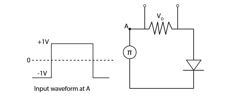
Draw the output waveform across the resistor in the figure.

Exemplar Solutions Class 12 Physics Chapter 14 - 8

14.21 The amplifiers X, Y and Z are connected in series. If the voltage gains of X, Y and Z are 10, 20 and 30, respectively and the input signal is 1 mV peak value, then what is the output signal voltage (peak value) (i) if dc supply voltage is 10V?

(ii) if dc supply voltage is 5V?

Show solutionHide solution
Worked solution

Voltage gain in X = vx = 10

Voltage gain in Y = vy = 20

Voltage gain in Z = vz = 30

Total voltage amplification = vx.vy.vz = 6V

i) If dc supply voltage is 10V then the output voltage is 6V

ii) If dc supply voltage is 5V then the output voltage will exceed 5V