My Cart
Your Cart 0

    Your cart is empty.

  • Total (Amount) ₹0.00
Previous year question hub

Digital Logic and Data Conversion - Analog and Digital Electronics - Electrical Engineering Previous Year Questions

Practice Digital Logic and Data Conversion - Analog and Digital Electronics - Electrical Engineering previous year questions organised from real papers, with year-wise coverage and clear topic navigation.

26Papers
19Years
76Questions
1Topics

Digital Logic and Data Conversion question pattern

Every graph below is calculated only from this selection.

Questions by year

Compare question counts across years.

Difficulty distribution

How the classified questions are distributed by difficulty.

Medium 46 60.5%
Easy 27 35.5%
Hard 3 3.9%
Question type distribution

MCQ, numerical, multiple-select and other formats found in these papers.

MCQ 68 89.5%
Numerical Answer Type (NAT) 8 10.5%

Subject weightage

Top subjects by unique question coverage.

Electrical Engineering
76 Qs

Most asked topics

Top topics across the included previous year papers.

Analog and Digital Electronics
76 Qs

Subtopic coverage

Top subtopics inside this exact selection.

Digital Logic and Data Conversion
76 Qs

Paper coverage

Question coverage for the most populated papers. Every active PYP paper remains listed below.

Electrical Engineering (EE) 2026
2 Qs
Electrical Engineering (EE) 2025
1 Qs
Electrical Engineering (EE) 2024
3 Qs
Electrical Engineering (EE) 2023
3 Qs
Electrical Engineering (EE) 2022
2 Qs
Electrical Engineering (EE) 2021
2 Qs
Electrical Engineering (EE) 2020
3 Qs
Electrical Engineering (EE) 2019
2 Qs
Electrical Engineering (EE) 2018
3 Qs
Electrical Engineering (EE) 2017 [Session 1]
3 Qs
Electrical Engineering (EE) 2017 [Session 2]
2 Qs
Electrical Engineering (EE) 2016 [Session 1]
3 Qs
Electrical Engineering (EE) 2016 [Session 2]
2 Qs
Electrical Engineering (EE) 2014 [Session 2]
4 Qs
Electrical Engineering (EE) 2014 [Session 1]
3 Qs
Electrical Engineering (EE) 2014 [Session 3]
3 Qs
Electrical Engineering (EE) 2013 [Session 1]
3 Qs
Electrical Engineering (EE) 2013 [Session 2]
3 Qs
Electrical Engineering (EE) 2013 [Session 4]
3 Qs
Electrical Engineering (EE) 2013 [Session 3]
2 Qs
Electrical Engineering (EE) 2012
4 Qs
Electrical Engineering (EE) 2011
3 Qs
Electrical Engineering (EE) 2010
4 Qs
Electrical Engineering (EE) 2009
3 Qs
Electrical Engineering (EE) 2008
5 Qs
Electrical Engineering (EE) 2007
5 Qs

Included previous year papers

Newest papers appear first. Search these papers or sort by year and name.

Paper nameYearPDFAttempt
Electrical Engineering (EE) 20262026
2 questions in this view
2026
Electrical Engineering (EE) 20252025
1 questions in this view
2025
Electrical Engineering (EE) 20242024
3 questions in this view
2024
Electrical Engineering (EE) 20232023
3 questions in this view
2023
Electrical Engineering (EE) 20222022
2 questions in this view
2022
Electrical Engineering (EE) 20212021
2 questions in this view
2021
Electrical Engineering (EE) 20202020
3 questions in this view
2020
Electrical Engineering (EE) 20192019
2 questions in this view
2019
Electrical Engineering (EE) 20182018
3 questions in this view
2018
Electrical Engineering (EE) 2017 [Session 1]2017
3 questions in this view
2017
Electrical Engineering (EE) 2017 [Session 2]2017
2 questions in this view
2017
Electrical Engineering (EE) 2016 [Session 1]2016
3 questions in this view
2016
Electrical Engineering (EE) 2016 [Session 2]2016
2 questions in this view
2016
Electrical Engineering (EE) 2014 [Session 1]2014
3 questions in this view
2014
Electrical Engineering (EE) 2014 [Session 2]2014
4 questions in this view
2014
Electrical Engineering (EE) 2014 [Session 3]2014
3 questions in this view
2014
Electrical Engineering (EE) 2013 [Session 1]2013
3 questions in this view
2013
Electrical Engineering (EE) 2013 [Session 2]2013
3 questions in this view
2013
Electrical Engineering (EE) 2013 [Session 3]2013
2 questions in this view
2013
Electrical Engineering (EE) 2013 [Session 4]2013
3 questions in this view
2013
Electrical Engineering (EE) 20122012
4 questions in this view
2012
Electrical Engineering (EE) 20112011
3 questions in this view
2011
Electrical Engineering (EE) 20102010
4 questions in this view
2010
Electrical Engineering (EE) 20092009
3 questions in this view
2009
Electrical Engineering (EE) 20082008
5 questions in this view
2008
Electrical Engineering (EE) 20072007
5 questions in this view
2007

All Digital Logic and Data Conversion previous year questions

Practice every matching question in batches of 20, with every available option.

1
2007 · Electrical Engineering · Analog and Digital Electronics · Digital Logic and Data Conversion
Electrical Engineering (EE) 2007

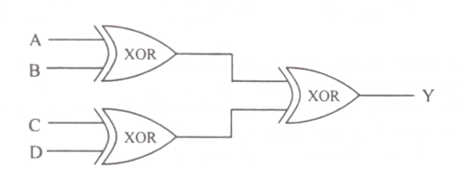
A, B, C and D are input bits, and Y is the output bit in the XOR gate circuit of the figure below. Which of the following statements about the sum S of A, B, C, D and Y is correct?

Question diagram

Open complete paper
2
2007 · Electrical Engineering · Analog and Digital Electronics · Digital Logic and Data Conversion
Electrical Engineering (EE) 2007

The octal equivalent of the HEX number AB.CD is

Open complete paper
3
2007 · Electrical Engineering · Analog and Digital Electronics · Digital Logic and Data Conversion
Electrical Engineering (EE) 2007

Which one of the following statements regarding the INT (interrupt) and the BRQ (bus request) pins in a CPU is true?

Open complete paper
4
2007 · Electrical Engineering · Analog and Digital Electronics · Digital Logic and Data Conversion
Electrical Engineering (EE) 2007
Suppose Reg contains the 2's complement number 11010110. If this number is divided by 2 the answer should be

Question diagram

Open complete paper
5
2007 · Electrical Engineering · Analog and Digital Electronics · Digital Logic and Data Conversion
Electrical Engineering (EE) 2007

Such a division can be correctly performed by the following set of operations

Open complete paper
6
2008 · Electrical Engineering · Analog and Digital Electronics · Digital Logic and Data Conversion
Electrical Engineering (EE) 2008

An input device is interfaced with Intel 8085A microprocessor as memory mapped I/O. The address of the device is 2500H. In order to input data from the device to accumulator, the sequence of instructions will be

Open complete paper
7
2008 · Electrical Engineering · Analog and Digital Electronics · Digital Logic and Data Conversion
Electrical Engineering (EE) 2008
A 3 line to 8 line decoder, with active low outputs, is used to implement a 3-variable Boolean function as shown in the figure. The simplified form of Boolean function F(A,B,C) implemented in ‘Product of Sum’ form will be
Open complete paper
8
2008 · Electrical Engineering · Analog and Digital Electronics · Digital Logic and Data Conversion
Electrical Engineering (EE) 2008
The truth table of a monoshot shown in the figure is given in the table below: [Table]. Two monoshots, one positive edge triggered and other negative edge triggered, are connected as shown in the figure. The pulse widths of the two monoshot outputs, \( Q_1 \) and \( Q_2 \), are \( T_{ON1} \) and \( T_{ON2} \), respectively. The frequency and the duty cycle of the signal at \( Q_1 \) will respectively be
Open complete paper
9
2008 · Electrical Engineering · Analog and Digital Electronics · Digital Logic and Data Conversion
Electrical Engineering (EE) 2008
The contents (in Hexadecimal) of some of the memory locations in an 8085A based system are given below: [Table]. The contents of stack pointer (SP), program counter (PC) and (H,L) are 2700H, 2100H and 0000H respectively. When the following sequence of instructions are executed, 2100 H: DAD SP ; 2101 H: PCHL ; the contents of (SP) and (PC) at the end of execution will be
Open complete paper
10
2008 · Electrical Engineering · Analog and Digital Electronics · Digital Logic and Data Conversion
Electrical Engineering (EE) 2008
The charge stored in the capacitor at t = 5 μs, will be

Question diagram

Open complete paper
11
2009 · Electrical Engineering · Analog and Digital Electronics · Digital Logic and Data Conversion
Electrical Engineering (EE) 2009

The increasing order of speed of data access for the following devices is (i) Cache Memory (ii) CDROM (iii) Dynamic RAM (iv) Processor Registers (v) Magnetic Tape

Open complete paper
12
2009 · Electrical Engineering · Analog and Digital Electronics · Digital Logic and Data Conversion
Electrical Engineering (EE) 2009

The complete set of only those Logic Gates designated as Universal Gates is

Open complete paper
13
2009 · Electrical Engineering · Analog and Digital Electronics · Digital Logic and Data Conversion
Electrical Engineering (EE) 2009
In an 8085 microprocessor, the contents of the Accumulator, after the following instructions are executed will become
XRA A
MVIB F0H
SUB B
Open complete paper
14
2010 · Electrical Engineering · Analog and Digital Electronics · Digital Logic and Data Conversion
Electrical Engineering (EE) 2010

The TTL circuit shown in the figure is fed with the waveform X (also shown). All gates have equal propagation delay of 10 ns. The output Y of the circuit is

Question diagram

Open complete paper
15
2010 · Electrical Engineering · Analog and Digital Electronics · Digital Logic and Data Conversion
Electrical Engineering (EE) 2010
When a “CALL Addr” instruction is executed, the CPU carries out the following sequential operations internally:
Note: (R) means content of register R
((R)) means content of memory location pointed to by R
PC means Program Counter
SP means Stack Pointer
Open complete paper
16
2010 · Electrical Engineering · Analog and Digital Electronics · Digital Logic and Data Conversion
Electrical Engineering (EE) 2010
The following Karnaugh map represents a function F.
A minimized form of the function F is

Question diagram

Open complete paper
17
2010 · Electrical Engineering · Analog and Digital Electronics · Digital Logic and Data Conversion
Electrical Engineering (EE) 2010
Which of the following circuits is a realization of the above function F ?
Open complete paper
18
2011 · Electrical Engineering · Analog and Digital Electronics · Digital Logic and Data Conversion
Electrical Engineering (EE) 2011

The output Y of the logic circuit given below is

Question diagram

Open complete paper
19
2011 · Electrical Engineering · Analog and Digital Electronics · Digital Logic and Data Conversion
Electrical Engineering (EE) 2011
A portion of the main program to call a subroutine SUB in an 8085 environment is given below.
...
LXI D, DISP
LP: CALL SUB
...
It is desired that control be returned to LP + DISP + 3 when the RET instruction is executed in the subroutine. The set of instructions that precede the RET instruction in the subroutine are
Open complete paper
20
2011 · Electrical Engineering · Analog and Digital Electronics · Digital Logic and Data Conversion
Electrical Engineering (EE) 2011
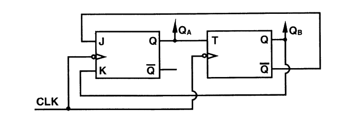
A two-bit counter circuit is shown below.
If the state \( Q_A Q_B \) of the counter at the clock time \( t_n \) is “10” then the state \( Q_A Q_B \) of the counter at \( t_n+3 \) (after three clock cycles) will be

Question diagram

Open complete paper

Showing 20 of 70 questions