My Cart
Your Cart 0

    Your cart is empty.

  • Total (Amount) ₹0.00
Previous year question hub

Power Semiconductor Devices - Power Electronics - Electrical Engineering Previous Year Questions

Practice Power Semiconductor Devices - Power Electronics - Electrical Engineering previous year questions organised from real papers, with year-wise coverage and clear topic navigation.

18Papers
14Years
30Questions
1Topics

Power Semiconductor Devices question pattern

Every graph below is calculated only from this selection.

Questions by year

Year-wise coverage for Power Semiconductor Devices. Each bar uses a separate theme-derived color.

Difficulty distribution

How the classified questions are distributed by difficulty.

Medium 22 73.3%
Easy 7 23.3%
Hard 1 3.3%
Question type distribution

MCQ, numerical, multiple-select and other formats found in these papers.

MCQ 22 73.3%
Numerical Answer Type (NAT) 5 16.7%
MSQ 3 10%

Subject weightage

Top subjects by unique question coverage.

Electrical Engineering
30 Qs

Most asked topics

Top topics across the included previous year papers.

Power Electronics
30 Qs

Subtopic coverage

Top subtopics inside this exact selection.

Power Semiconductor Devices
30 Qs

Paper coverage

Question coverage for the most populated papers. Every active PYP paper remains listed below.

Electrical Engineering (EE) 2024
1 Qs
Electrical Engineering (EE) 2023
2 Qs
Electrical Engineering (EE) 2022
1 Qs
Electrical Engineering (EE) 2020
1 Qs
Electrical Engineering (EE) 2018
1 Qs
Electrical Engineering (EE) 2017 [Session 1]
1 Qs
Electrical Engineering (EE) 2016 [Session 1]
2 Qs
Electrical Engineering (EE) 2014 [Session 1]
1 Qs
Electrical Engineering (EE) 2014 [Session 2]
1 Qs
Electrical Engineering (EE) 2013 [Session 1]
2 Qs
Electrical Engineering (EE) 2013 [Session 2]
2 Qs
Electrical Engineering (EE) 2013 [Session 3]
2 Qs
Electrical Engineering (EE) 2013 [Session 4]
2 Qs
Electrical Engineering (EE) 2012
1 Qs
Electrical Engineering (EE) 2011
2 Qs
Electrical Engineering (EE) 2010
2 Qs
Electrical Engineering (EE) 2009
3 Qs
Electrical Engineering (EE) 2007
3 Qs

Included previous year papers

Newest papers appear first. Sort by year, question coverage or name.

PaperYear / sessionQuestions in this viewOpen
Electrical Engineering (EE) 202420241View paper
Electrical Engineering (EE) 202320232View paper
Electrical Engineering (EE) 202220221View paper
Electrical Engineering (EE) 202020201View paper
Electrical Engineering (EE) 201820181View paper
Electrical Engineering (EE) 2017 [Session 1]20171View paper
Electrical Engineering (EE) 2016 [Session 1]20162View paper
Electrical Engineering (EE) 2014 [Session 1]20141View paper
Electrical Engineering (EE) 2014 [Session 2]20141View paper
Electrical Engineering (EE) 2013 [Session 1]20132View paper
Electrical Engineering (EE) 2013 [Session 2]20132View paper
Electrical Engineering (EE) 2013 [Session 3]20132View paper
Electrical Engineering (EE) 2013 [Session 4]20132View paper
Electrical Engineering (EE) 201220121View paper
Electrical Engineering (EE) 201120112View paper
Electrical Engineering (EE) 201020102View paper
Electrical Engineering (EE) 200920093View paper
Electrical Engineering (EE) 200720073View paper

All Power Semiconductor Devices previous year questions

Practice every matching question in batches of 20, with every available option.

1
2007 · Electrical Engineering · Power Electronics · Power Semiconductor Devices
Electrical Engineering (EE) 2007
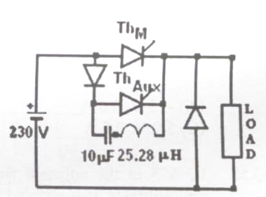
The circuit in the figure is a current commutated dc – dc chopper where, ThM is the main SCR and ThAUX is the auxiliary SCR. The load current is constant at 10 A. ThM is ON. ThAUX is triggered at t = 0. ThM is turned OFF between

Question diagram

Open complete paper
2
2007 · Electrical Engineering · Power Electronics · Power Semiconductor Devices
Electrical Engineering (EE) 2007
The resistance R should be

Question diagram

Open complete paper
3
2007 · Electrical Engineering · Power Electronics · Power Semiconductor Devices
Electrical Engineering (EE) 2007

The minimum approximate volt-second rating of the pulse transformer suitable for triggering the SCR should be: (volt-second rating is the maximum of product of the voltage and the width of the pulse that may be applied)

Open complete paper
4
2009 · Electrical Engineering · Power Electronics · Power Semiconductor Devices
Electrical Engineering (EE) 2009

An SCR is considered to be a semi-controlled device because

Open complete paper
5
2009 · Electrical Engineering · Power Electronics · Power Semiconductor Devices
Electrical Engineering (EE) 2009
The circuit shows an ideal diode connected to a pure inductor and is connected to a purely sinusoidal 50Hz voltage source. Under ideal conditions the current waveform through the inductor will look like
Open complete paper
6
2009 · Electrical Engineering · Power Electronics · Power Semiconductor Devices
Electrical Engineering (EE) 2009
In the chopper circuit shown, the main thyristor (TM) is operated at a duty ratio of 0.8 which is much larger the commutation interval. If the maximum allowable reapplied dv/dt on TM is 50 V/μs, what should be the theoretical minimum value of C1 ? Assume current ripple through L0 to be negligible.
Open complete paper
7
2010 · Electrical Engineering · Power Electronics · Power Semiconductor Devices
Electrical Engineering (EE) 2010

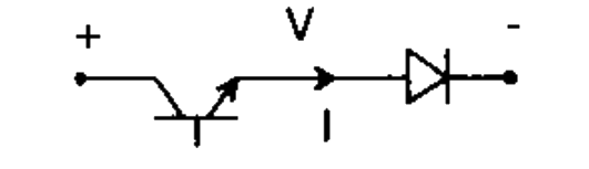
Figure shows a composite switch consisting of a power transistor (BJT) in series with a diode. Assuming that the transistor switch and the diode are ideal, the I-V characteristic of the composite switch is

Question diagram

Open complete paper
8
2010 · Electrical Engineering · Power Electronics · Power Semiconductor Devices
Electrical Engineering (EE) 2010

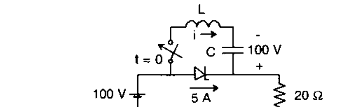
The L-C circuit of Q54 is used to commutate a thyristor, which is initially carrying a current of 5 A as shown in the figure below. The values and initial conditions of L and C are the same as in Q54. The switch is closed at t = 0. If the forward drop is negligible, the time taken for the device to turn off is

Question diagram

Open complete paper
9
2011 · Electrical Engineering · Power Electronics · Power Semiconductor Devices
Electrical Engineering (EE) 2011

Circuit turn-off time of an SCR is defined as the time

Open complete paper
10
2011 · Electrical Engineering · Power Electronics · Power Semiconductor Devices
Electrical Engineering (EE) 2011
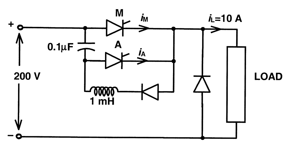
A voltage commutated chopper circuit, operated at 500Hz, is shown below. If the maximum value of load current is 10 A, then the maximum current through the main (M) and auxiliary (A) thyristors will be

Question diagram

Open complete paper
11
2012 · Electrical Engineering · Power Electronics · Power Semiconductor Devices
Electrical Engineering (EE) 2012
The typical ratio of latching current to holding current in a 20 A thyristor is
(A) 5.0
(B) 2.0
(C) 1.0
(D) 0.5
Open complete paper
12
2013 · Electrical Engineering · Power Electronics · Power Semiconductor Devices
Electrical Engineering (EE) 2013 [Session 1]
Thyristor T in the figure below is initially off and is triggered with a single pulse of width 10 \( \mu s \). It is given that \( L = \frac{100}{\pi} \mu H \) and \( C = \frac{100}{\pi} \mu F \). Assuming latching and holding currents of the thyristor are both zero and the initial charge on C is zero, T conducts for
Open complete paper
13
2013 · Electrical Engineering · Power Electronics · Power Semiconductor Devices
Electrical Engineering (EE) 2013 [Session 1]

Appropriate transition i.e., Zero Voltage Switching (ZVS)/Zero Current Switching (ZCS) of the IGBTs during turn-on/turn-off is

Open complete paper
14
2013 · Electrical Engineering · Power Electronics · Power Semiconductor Devices
Electrical Engineering (EE) 2013 [Session 2]
Thyristor T in the figure below is initially off and is triggered with a single pulse of width 10 µs. It is given that \( L = \left(\frac{100}{\pi}\right) \mu H \) and \( C = \left(\frac{100}{\pi}\right) \mu F \). Assuming latching and holding currents of the thyristor are both zero and the initial charge on C is zero, T conducts for
Open complete paper
15
2013 · Electrical Engineering · Power Electronics · Power Semiconductor Devices
Electrical Engineering (EE) 2013 [Session 3]
Thyristor T in the figure below is initially off and is triggered with a single pulse of width 10 \(\mu\)s. It is given that \(L=(\frac{100}{\pi})\mu\)H and \(C=(\frac{100}{\pi})\mu\)F. Assuming latching and holding currents of the thyristor are both zero and the initial charge on C is zero, T conducts for
Open complete paper
16
2013 · Electrical Engineering · Power Electronics · Power Semiconductor Devices
Electrical Engineering (EE) 2013 [Session 4]
Thyristor T in the figure below is initially off and is triggered with a single pulse of width 10 \(\mu\)s. It is given that \( L = \left(\frac{100}{\pi}\right)\mu H \) and \( C = \left(\frac{100}{\pi}\right)\mu F \). Assuming latching and holding currents of the thyristor are both zero and the initial charge on C is zero, T conducts for
Open complete paper
17
2014 · Electrical Engineering · Power Electronics · Power Semiconductor Devices
Electrical Engineering (EE) 2014 [Session 1]
Figure shows four electronic switches (i), (ii), (iii) and (iv). Which of the switches can block voltages of either polarity (applied between terminals 'a' and 'b') when the active device is in the OFF state?
Open complete paper
18
2014 · Electrical Engineering · Power Electronics · Power Semiconductor Devices
Electrical Engineering (EE) 2014 [Session 2]
The SCR in the circuit shown has a latching current of 40 mA. A gate pulse of 50 μs is applied to the SCR. The maximum value of R in Ω to ensure successful firing of the SCR is ________.

Question diagram

Open complete paper
19
2016 · Electrical Engineering · Power Electronics · Power Semiconductor Devices
Electrical Engineering (EE) 2016 [Session 1]
A steady dc current of 100 A is flowing through a power module (S, D) as shown in Figure (a). The V-I characteristics of the IGBT (S) and the diode (D) are shown in Figures (b) and (c), respectively. The conduction power loss in the power module (S, D), in watts, is ______
Open complete paper
20
2016 · Electrical Engineering · Power Electronics · Power Semiconductor Devices
Electrical Engineering (EE) 2016 [Session 1]
The voltage \(v_s\) across and the current \(i_s\) through a semiconductor switch during a turn-ON transition are shown in figure. The energy dissipated during the turn-ON transition, in mJ, is ________.
Open complete paper

Showing 20 of 27 questions