Difficulty distribution
How the classified questions are distributed by difficulty.
37questions
Not classified
37
100%
Your cart is empty.
Practice Semiconductor Devices And Logic Gates - Modern Physics - Physics previous year questions organised from real papers, with year-wise coverage and clear topic navigation.
Every graph below is calculated only from this selection.
Year-wise coverage for Semiconductor Devices And Logic Gates. Each bar uses a separate theme-derived color.
How the classified questions are distributed by difficulty.
MCQ, numerical, multiple-select and other formats found in these papers.
Top subjects by unique question coverage.
Top topics across the included previous year papers.
Top subtopics inside this exact selection.
Question coverage for the most populated papers. Every active PYP paper remains listed below.
Newest papers appear first. Sort by year, question coverage or name.
| Paper | Year / session | Questions in this view | Open |
|---|---|---|---|
| COMEDK 2026 Afternoon Shift | 2026 | 3 | View paper |
| COMEDK 2026 Morning Shift | 2026 | 3 | View paper |
| COMEDK 2025 AFTERNOON SHIFT | 2025 | 3 | View paper |
| COMEDK 2025 EVENING SHIFT | 2025 | 3 | View paper |
| COMEDK 2025 Morning Shift | 2025 | 3 | View paper |
| COMEDK 2024 AFTERNOON SHIFT | 2024 | 4 | View paper |
| COMEDK 2024 EVENING SHIFT | 2024 | 3 | View paper |
| COMEDK 2024 MORNING SHIFT | 2024 | 3 | View paper |
| COMEDK 2023 EVENING SHIFT | 2023 | 3 | View paper |
| COMEDK 2023 Morning Shift | 2023 | 3 | View paper |
| COMEDK 2022 | 2022 | 3 | View paper |
| COMEDK 2021 | 2021 | 2 | View paper |
| COMEDK 2020 | 2020 | 1 | View paper |
Practice every matching question in batches of 20, with every available option.
When a \(p\)-\(n\) junction diode is connected in forward bias, its barrier potential
Find the logic gate, when both the inputs are high but the output is low and vice-versa.
What is the minimum band-gap of the LED diode?
For CE transistor amplifier, the audio signal voltage across the collector resistance of 4 k\(\Omega\) is 5 V. If the current amplification factor of the transistor is 100 and base resistance is 2 k\(\Omega\), then input signal voltage is
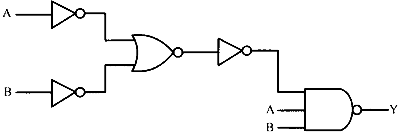
Which of the following gate give the similar output as the output of circuit diagram shown in the figure?
Choose the incorrect statements.
The energy gap between valance band and the conduction band for a given material is \(6 \mathrm{~eV}\), then the material is :
In the given circuit the diode \(D_1\) and \(D_2\) have the forward resistance \(25 \Omega\) and infinite backward resistance. When they are connected to the source as shown, the current passing through the \(175 \Omega\) resistor is:

The reverse current in the semiconductor diode changes from \(20 \mu \mathrm{A}\) to \(40 \mu \mathrm{A}\) when the reverse potential is changed from \(10 \mathrm{~V}\) to \(15 \mathrm{~V}\), then the reverse resistance of the junction diode will be :
The mobility of the charge carriers increases with
$$\text { In a p-n junction, the depletion layer of thickness } 1 \mu \mathrm{m} \text { has } 0.05 \mathrm{~V} \text { potential across it. The electric field in } N C^{-1} \text { is }$$
In intrinsic semiconductors at room temperature, number of electrons and holes are
A semiconductor \(\mathrm{X}\) is made by doping silicon with phosphorous. A second semiconductor \(\mathrm{Y}\) is made by doping silicon with aluminium. The two are joined by a suitable technique to form a \(\mathrm{p}\)-\(\mathrm{n}\) junction and is connected to a battery such that \(\mathrm{Y}\) is joined to negative of the battery and \(\mathrm{X}\) to the positive of the battery. Which of the following statements is correct?
The conductivity of a semiconductor increases with increase in temperature because
A) number density of free current carriers increases
B) relaxation time increases
C) both number density of carriers and relaxation time increase
D) number density of current carriers increases, relaxation time decreases but effect of decrease in relaxation time is much less than increase in number density
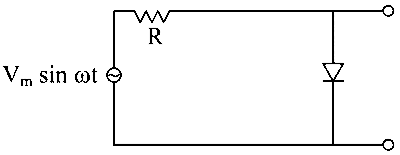
The output of the given circuit is
A. Negatively rectified half wave
B. Positively rectified half wave
C. Negatively rectified full wave
D. Zero all times
The following are the graphs of potential barrier versus width of the depletion region for a p-n junction diode.
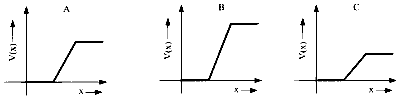
Which of the following is correct?
| I | II | III | IV` |
|---|---|---|---|
| A - unbiased diode | A - Forward biased diode | A - unbiased diode | A - unbiased diode |
| B - Reverse biased | B - Reverse biased | B - Forward biased | B - unused diode |
| C - Forward biased | C - unbiased | C - Reverse biased | C - Forward biased |
Though \(\mathrm{Sn}\) and \(\mathrm{Si}\) are \(4^{\text {th }}\) group elements, \(\mathrm{Sn}\) is a metal while \(\mathrm{Si}\) is a semiconductor because
In a given semiconductor, the ratio of the number density of electron to number density of hole is \(2: 1\). If \(\frac{1}{7}\)th of the total current is due to the hole and the remaining is due to the electrons, the ratio of the drift velocity of holes to the drift velocity of electrons is :
An ideal diode is connected in series with a capacitor. The free ends of the capacitor and the diode are connected across a \(220 \mathrm{~V}\) ac source. Now the potential difference across the capacitor is :
Showing 20 of 37 questions