My Cart
Your Cart 0

    Your cart is empty.

  • Total (Amount) ₹0.00
NCERT Exemplar · Class 12 · Physics

Chapter 14: Semiconductor Electronics: Materials, Devices and Simple Circuits

Practice each question, then open the answer or worked solution.

Questions

38 questions
Q14.32Written answer

In the circuit shown in the figure, when the input voltage of the base resistance is 10V, Vbe is zero and Vce is also zero. Find the values of Ib, Ic and β.
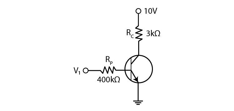
Exemplar Solutions Class 12 Physics Chapter 14 - 15

Show solutionHide solution
Worked solution

Vi = 10 V

Rb = 400 kilo ohms

Vbe = 0

Vce = 0

Rc = 3 kilo ohms

Ib = 25 micro ampere

Rc = 10 V

Ic = 3.33 mA

Current gain = 133
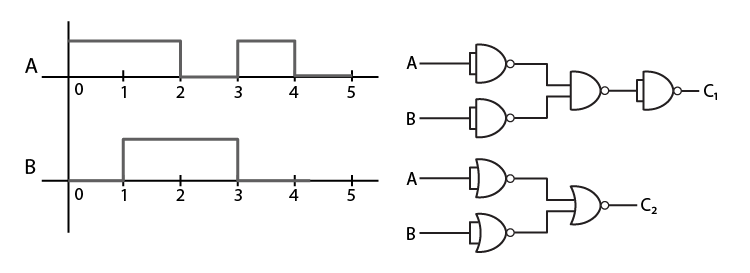
Q14.33Written answer

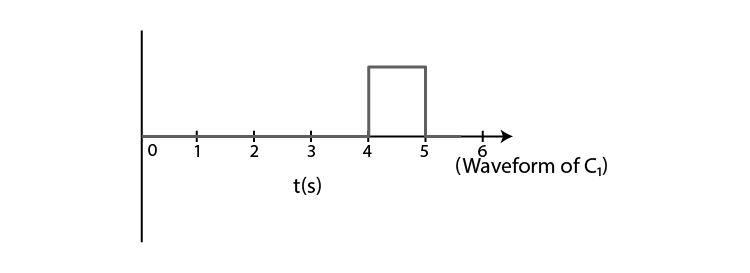
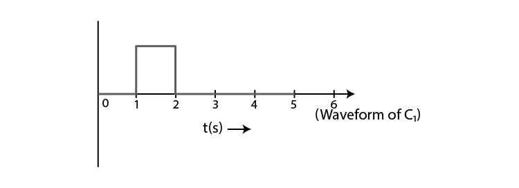
Draw the output signals C1 and C2 in the given combination of gates in the figure.

Exemplar Solutions Class 12 Physics Chapter 14 - 16

Exemplar Solutions Class 12 Physics Chapter 14 - 17

Exemplar Solutions Class 12 Physics Chapter 14 - 18

14.34 Consider the circuit arrangement in which the input and output characteristics of NPN transistor in CE configuration

Select the values of RB and RC for a transistor whose VBE = 0.7 V, so that the transistor is operating at point Q as shown in the characteristics shown in the figure (b). Given that the input impedance of the transistor is very small and VCC = VBB = 16 V, also find the voltage gain and power gain of circuit making appropriate assumptions.

Show solutionHide solution
Worked solution

Vbe = 0.7V

Vcc = Vbb = 16V

Vce = 8V

Ic = 4 mA = 4 × 10⁻³ A

Ib = 30 × 10-6 A

Rc = 2 kilo ohms

Rb = 510 kilo ohms

Current gain = 1333

Voltage gain = 0.52

Power gain = 69

Q14.35Written answer

Assuming the ideal diode. Explain the waveform.

Show solutionHide solution
Worked solution

The waveform of the above circuit would be a sine wave with a dip off in the input wave.

Q14.36Written answer

Suppose a ‘n’-type wafer is created by doping Si crystal having 5 × 1028 atoms/m3 with 1ppm concentration of As. On the surface 200 ppm Boron is added to create the ‘P’ region in this wafer. Considering ni = 1.5 × 10¹⁶ m–3,

(i) Calculate the densities of the charge carriers in the n & p regions.

(ii) Comment which charge carriers would contribute largely for the reverse saturation current when the diode is reverse biased.

Show solutionHide solution
Worked solution

i) Ne = 5 × 10²² m3

Nh = 0.45 × 10¹⁰ m3

Nh = Na = 1 × 1025 m3

Ne = 2.25 × 10⁷ m3

ii) The minority carrier holes of n-region would contribute largely for the reverse saturation current when the diode is reverse biased.

Q14.37Written answer

An X-OR gate has the following truth table:

A B Y
0 0 0
0 1 1
1 0 1
1 1 0

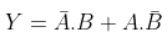
It is represented by the following logic relation

Exemplar Solutions Class 12 Physics Chapter 14 - 19

Build this gate using AND, OR, and NOT gates.

Show solutionHide solution
Worked solution

The logic relation is y = A.B + A.B

Q14.38Multiple choice

Consider a box with three terminals on top of it:

Three components namely, two germanium diodes and one resistor are connected across these three terminals in some arrangement. A student performs an experiment in which any two of these three terminals are connected in the circuit shown in the figure (b).

The student obtains graphs of current-voltage characteristics for an unknown combination of components between the two terminals connected in the circuit.

The graphs are

(v) When A is positive and C is negative

(vi) When A is negative and C is positive

From these graphs of current-voltage characteristic shown in the figures, determine the arrangement of components between A, B and C.

Show solutionHide solution
Worked solution

a) A is connected to the n-side of the PN junction and B is connected to the top-side of pn junction.

b) 0.7 V is the knee voltage.

c) Pn junction is connected to C and n-side of pn junction to B and knee voltage is 0.7 V.

d) The above conditions explains the connection of pn-junction along I and II with the resistance.

Q14.39Written answer

For the transistor circuit shown in Fig.14.19, evaluate VE, RB, RE given IC = 1 mA, VCE = 3V, VBE = 0.5 V and VCC = 12 V, β = 100.

Show solutionHide solution
Worked solution

Ic = Ie

Rc = 7.8 kilo ohm

Ic (Rc + Re) + Vce = 12

Ve = 1.2 V

Vb = Ve + Vbe = 1.7 V

I = 0.085 mA

Rb = 108 kilo ohms

Q14.40Written answer

In the circuit, find the value of RC.

Show solutionHide solution
Worked solution

Ie = Ic + Ib

IcRc + Vce + IeRe = Vcc

Rib + Vbe + IeRe = Vcc

Ib = 11.5/200 mA

Rc + Re = 1.56 kilo ohm

Rc = 560 Ohm

Semiconductor electronics refers to the different electronic circuits, components and devices that are made with a different kind of material, unlike metals and non-metals. Materials based on resistivity and conductivity are categorised into metals, non-metals and semiconductors. They have a wide range of applications, especially in the field of conducting and resisting electricity. Other topics discussed in this chapter are

  1. Digital electronics
  2. Logic gates
  3. Intrinsic and extrinsic semiconductor
  4. P-n junction
  5. Junction diode as a rectifier