My Cart
Your Cart 0

    Your cart is empty.

  • Total (Amount) ₹0.00
Previous year question hub

Semiconductor Energy Bands and Carrier Statistics - Electronic Devices - Electronics & Communication Engineering Previous Year Questions

Practice Semiconductor Energy Bands and Carrier Statistics - Electronic Devices - Electronics & Communication Engineering previous year questions organised from real papers, with year-wise coverage and clear topic navigation.

10Papers
10Years
14Questions
1Topics

Semiconductor Energy Bands and Carrier Statistics question pattern

Every graph below is calculated only from this selection.

Questions by year

Compare question counts across years.

Difficulty distribution

How the classified questions are distributed by difficulty.

Easy 8 57.1%
Medium 6 42.9%

Question type distribution

MCQ, numerical, multiple-select and other formats found in these papers.

MCQ 13 92.9%
Numerical Answer Type (NAT) 1 7.1%

Subject weightage

Top subjects by unique question coverage.

Electronics & Communication Engineering
14 Qs

Most asked topics

Top topics across the included previous year papers.

Electronic Devices
14 Qs

Subtopic coverage

Top subtopics inside this exact selection.

Semiconductor Energy Bands and Carrier Statistics
14 Qs

Paper coverage

Question coverage for the most populated papers. Every active PYP paper remains listed below.

Electronics & Communication Engineering (EC) 2024
1 Qs
Electronics & Communication Engineering (EC) 2023
3 Qs
Electronics & Communication Engineering (EC) 2022
1 Qs
Electronics & Communication Engineering (EC) 2021
1 Qs
Electronics & Communication Engineering (EC) 2020
1 Qs
Electronics & Communication Engineering (EC) 2016 [Session 1]
1 Qs
Electronics & Communication Engineering (EC) 2014 [Session 4]
2 Qs
Electronics & Communication Engineering (EC) 2012
1 Qs
Electronics & Communication Engineering (EC) 2009
1 Qs
Electronics & Communication Engineering (EC) 2008
2 Qs

Included previous year papers

Newest papers appear first. Search these papers or sort by year and name.

Paper nameYearPDFAttempt
Electronics & Communication Engineering (EC) 20242024
1 questions in this view
2024
Electronics & Communication Engineering (EC) 20232023
3 questions in this view
2023
Electronics & Communication Engineering (EC) 20222022
1 questions in this view
2022
Electronics & Communication Engineering (EC) 20212021
1 questions in this view
2021
Electronics & Communication Engineering (EC) 20202020
1 questions in this view
2020
Electronics & Communication Engineering (EC) 2016 [Session 1]2016
1 questions in this view
2016
Electronics & Communication Engineering (EC) 2014 [Session 4]2014
2 questions in this view
2014
Electronics & Communication Engineering (EC) 20122012
1 questions in this view
2012
Electronics & Communication Engineering (EC) 20092009
1 questions in this view
2009
Electronics & Communication Engineering (EC) 20082008
2 questions in this view
2008

All Semiconductor Energy Bands and Carrier Statistics previous year questions

Practice every matching question in batches of 20, with every available option.

1
2008 · Electronics & Communication Engineering · Electronic Devices · Semiconductor Energy Bands and Carrier Statistics
Electronics & Communication Engineering (EC) 2008

Which of the following is true?

Open complete paper
2
2008 · Electronics & Communication Engineering · Electronic Devices · Semiconductor Energy Bands and Carrier Statistics
Electronics & Communication Engineering (EC) 2008
Silicon is doped with boron to a concentration of $4 \times 10^{17}$ atoms/cm³. Assume the intrinsic carrier concentration of silicon to be $1.5 \times 10^{10}$/cm³ and the value of $\frac{kT}{q}$ to be 25 mV at 300 K. Compared to undoped silicon, the Fermi level of doped silicon
Open complete paper
3
2009 · Electronics & Communication Engineering · Electronic Devices · Semiconductor Energy Bands and Carrier Statistics
Electronics & Communication Engineering (EC) 2009
In an n-type silicon crystal at room temperature, which of the following can have a concentration of \(4 \times 10^{19} \text{ cm}^{-3}\) ?
Open complete paper
4
2012 · Electronics & Communication Engineering · Electronic Devices · Semiconductor Energy Bands and Carrier Statistics
Electronics & Communication Engineering (EC) 2012
The source of a silicon (\( n_i = 10^{10} \) per \( cm^3 \)) n-channel MOS transistor has an area of 1 sq \( \mu m \) and a depth of 1 \( \mu m \). If the dopant density in the source is \( 10^{19}/cm^3 \), the number of holes in the source region with the above volume is approximately
Open complete paper
5
2014 · Electronics & Communication Engineering · Electronic Devices · Semiconductor Energy Bands and Carrier Statistics
Electronics & Communication Engineering (EC) 2014 [Session 4]
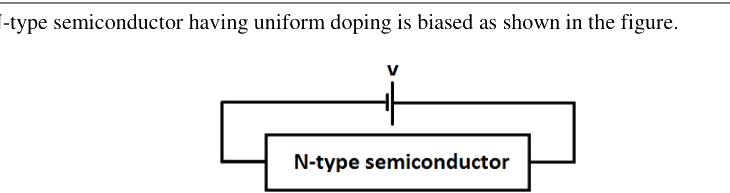
An N-type semiconductor having uniform doping is biased as shown in the figure.
If EC is the lowest energy level of the conduction band, EV is the highest energy level of the valance band and EF is the Fermi level, which one of the following represents the energy band diagram for the biased N-type semiconductor?

Question diagram

Open complete paper
6
2014 · Electronics & Communication Engineering · Electronic Devices · Semiconductor Energy Bands and Carrier Statistics
Electronics & Communication Engineering (EC) 2014 [Session 4]
At T = 300 K, the band gap and the intrinsic carrier concentration of GaAs are 1.42 eV and \(10^6\) cm\(^{-3}\), respectively. In order to generate electron hole pairs in GaAs, which one of the wavelength (\(\lambda_c\)) ranges of incident radiation, is most suitable? (Given that: Plank's constant is \(6.62 \times 10^{-34}\) J-s, velocity of light is \(3 \times 10^{10}\) cm/s and charge of electron is \(1.6 \times 10^{-19}\) C)
Open complete paper
7
2016 · Electronics & Communication Engineering · Electronic Devices · Semiconductor Energy Bands and Carrier Statistics
Electronics & Communication Engineering (EC) 2016 [Session 1]
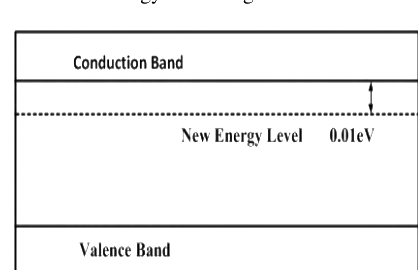
A small percentage of impurity is added to an intrinsic semiconductor at 300 K. Which one of the following statements is true for the energy band diagram shown in the following figure?

Question diagram

Open complete paper
8
2020 · Electronics & Communication Engineering · Electronic Devices · Semiconductor Energy Bands and Carrier Statistics
Electronics & Communication Engineering (EC) 2020
A single crystal intrinsic semiconductor is at a temperature of 300 K with effective density of states for holes twice that of electrons. The thermal voltage is 26 mV. The intrinsic Fermi level is shifted from mid-bandgap energy level by
Open complete paper
9
2021 · Electronics & Communication Engineering · Electronic Devices · Semiconductor Energy Bands and Carrier Statistics
Electronics & Communication Engineering (EC) 2021
The energy band diagram of a p-type semiconductor bar of length \(L\) under equilibrium condition (i.e., the Fermi energy level \(E_F\) is constant) is shown in the figure. The valence band \(E_V\) is sloped since doping is non-uniform along the bar. The difference between the energy levels of the valence band at the two edges of the bar is \(\Delta\).
If the charge of an electron is \(q\), then the magnitude of the electric field developed inside this semiconductor bar is
Open complete paper
10
2022 · Electronics & Communication Engineering · Electronic Devices · Semiconductor Energy Bands and Carrier Statistics
Electronics & Communication Engineering (EC) 2022
In a non-degenerate bulk semiconductor with electron density \(n = 10^{16} \text{ cm}^{-3}\), the value of \(E_C - E_{Fn} = 200 \text{ meV}\), where \(E_C\) and \(E_{Fn}\) denote the bottom of the conduction band energy and electron Fermi level energy, respectively. Assume thermal voltage as 26 meV and the intrinsic carrier concentration is \(10^{10} \text{ cm}^{-3}\). For \(n = 0.5 \times 10^{16} \text{ cm}^{-3}\), the closest approximation of the value of \((E_C - E_{Fn})\), among the given options, is ________.
Open complete paper
11
2023 · Electronics & Communication Engineering · Electronic Devices · Semiconductor Energy Bands and Carrier Statistics
Electronics & Communication Engineering (EC) 2023

In a semiconductor, if the Fermi energy level lies in the conduction band, then the semiconductor is known as

Open complete paper
12
2023 · Electronics & Communication Engineering · Electronic Devices · Semiconductor Energy Bands and Carrier Statistics
Electronics & Communication Engineering (EC) 2023
For an intrinsic semiconductor at temperature \( T = 0 K \), which of the following statement is true?
Open complete paper
13
2023 · Electronics & Communication Engineering · Electronic Devices · Semiconductor Energy Bands and Carrier Statistics
Electronics & Communication Engineering (EC) 2023
In a semiconductor device, the Fermi-level energy is 0.35 eV above the valence band energy. The effective density of states in the valence band at \(T = 300\) K is \(1 \times 10^{19} cm^{-3}\). The thermal equilibrium hole concentration in silicon at 400 K is ______ \(\times 10^{13} cm^{-3}\) (rounded off to two decimal places). Given \(kT\) at 300 K is 0.026 eV.
Open complete paper
14
2024 · Electronics & Communication Engineering · Electronic Devices · Semiconductor Energy Bands and Carrier Statistics
Electronics & Communication Engineering (EC) 2024
For non-degenerately doped n-type silicon, which one of the following plots represents the temperature (\( T \)) dependence of free electron concentration (\( n \))?
Open complete paper