BJT and MOSFET Amplifiers - Analog Circuits - Electronics & Communication Engineering Previous Year Questions
Practice BJT and MOSFET Amplifiers - Analog Circuits - Electronics & Communication Engineering previous year questions organised from real papers, with year-wise coverage and clear topic navigation.
29Papers
19Years
75Questions
1Topics
BJT and MOSFET Amplifiers question pattern
Every graph below is calculated only from this selection.
Questions by year
Compare question counts across years.
Difficulty distribution
How the classified questions are distributed by difficulty.
75questions
Medium57
76%
Easy10
13.3%
Hard8
10.7%
Question type distribution
MCQ, numerical, multiple-select and other formats found in these papers.
75questions
MCQ55
73.3%
Numerical Answer Type (NAT)13
17.3%
Fill in the blanks4
5.3%
MSQ3
4%
Subject weightage
Top subjects by unique question coverage.
Electronics & Communication Engineering
75 Qs
Most asked topics
Top topics across the included previous year papers.
Analog Circuits
75 Qs
Subtopic coverage
Top subtopics inside this exact selection.
BJT and MOSFET Amplifiers
75 Qs
Paper coverage
Question coverage for the most populated papers. Every active PYP paper remains listed below.
Electronics and Communication Engineering (EC) 2026
2 Qs
Electronics & Communication Engineering (EC) 2025
5 Qs
Electronics & Communication Engineering (EC) 2024
2 Qs
Electronics & Communication Engineering (EC) 2023
3 Qs
Electronics & Communication Engineering (EC) 2022
3 Qs
Electronics & Communication Engineering (EC) 2021
2 Qs
Electronics & Communication Engineering (EC) 2020
1 Qs
Electronics & Communication Engineering (EC) 2019
2 Qs
Electronics & Communication Engineering (EC) 2018
1 Qs
Electronics & Communication Engineering (EC) 2017 [Session 2]
4 Qs
Electronics & Communication Engineering (EC) 2017
3 Qs
Electronics & Communication Engineering (EC) 2017 [Session 1]
3 Qs
Electronics & Communication Engineering (EC) 2016 [Session 3]
3 Qs
Electronics & Communication Engineering (EC) 2016 [Session 2]
2 Qs
Electronics & Communication Engineering (EC) 2016 [Session 1]
1 Qs
Electronics & Communication Engineering (EC) 2014 [Session 4]
4 Qs
Electronics & Communication Engineering (EC) 2014 [Session 1]
2 Qs
Electronics & Communication Engineering (EC) 2014 [Session 2]
1 Qs
Electronics & Communication Engineering (EC) 2014 [Session 3]
1 Qs
Electronics & Communication Engineering (EC) 2013 [Session 2]
3 Qs
Electronics & Communication Engineering (EC) 2013 [Session 3]
3 Qs
Electronics & Communication Engineering (EC) 2013 [Session 1]
2 Qs
Electronics & Communication Engineering (EC) 2013 [Session 4]
2 Qs
Electronics & Communication Engineering (EC) 2012
3 Qs
Electronics & Communication Engineering (EC) 2011
4 Qs
Electronics & Communication Engineering (EC) 2010
3 Qs
Electronics & Communication Engineering (EC) 2009
3 Qs
Electronics & Communication Engineering (EC) 2008
4 Qs
Electronics & Communication Engineering (EC) 2007
3 Qs
Included previous year papers
Newest papers appear first. Search these papers or sort by year and name.
Paper name
Year
PDF
Attempt
Electronics and Communication Engineering (EC) 20262026
2007 · Electronics & Communication Engineering · Analog Circuits · BJT and MOSFET Amplifiers
Electronics & Communication Engineering (EC) 2007
For the BJT circuit shown, assume that the \(\beta\) of the transistor is very large and \(V_{BE} = 0.7\text{ V}\). The mode of operation of the BJT is
2007 · Electronics & Communication Engineering · Analog Circuits · BJT and MOSFET Amplifiers
Electronics & Communication Engineering (EC) 2007
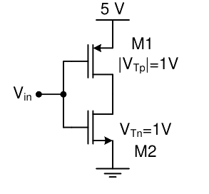
In the CMOS inverter circuit shown, if the transconductance parameters of the NMOS and PMOS transistors are \(k_n = k_p = \mu_n C_{ox} \frac{W_n}{L_n} = \mu_p C_{ox} \frac{W_p}{L_p} = 40 \text{ }\mu\text{A/V}^2\) and their threshold voltages are \(V_{THn} = |V_{THp}| = 1\text{ V}\), the current \(I\) is
2008 · Electronics & Communication Engineering · Analog Circuits · BJT and MOSFET Amplifiers
Electronics & Communication Engineering (EC) 2008
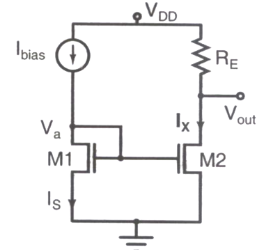
For the circuit shown in the following figure, transistors M1 and M2 are identical NMOS transistors. Assume that M2 is in saturation and the output is unloaded.\n\nThe current \(I_X\) is related to \(I_{bias}\) as
2008 · Electronics & Communication Engineering · Analog Circuits · BJT and MOSFET Amplifiers
Electronics & Communication Engineering (EC) 2008
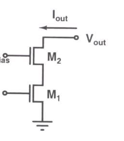
Two identical NMOS transistors M1 and M2 are connected as shown below. $V_{bias}$ is chosen so that both transistors are in saturation. The equivalent $g_m$ of the pair is defined to be $\frac{\partial I_{out}}{\partial V_i}$ at constant $V_{out}$. The equivalent $g_m$ of the pair is
2009 · Electronics & Communication Engineering · Analog Circuits · BJT and MOSFET Amplifiers
Electronics & Communication Engineering (EC) 2009
A small signal source \(v_i(t) = A\cos 20t + B\sin 10^6 t\) is applied to a transistor amplifier as shown below. The transistor has \(\beta = 150\) and \(h_{ie} = 3\text{k}\Omega\). Which expression best approximates \(v_o(t)\) ?
2010 · Electronics & Communication Engineering · Analog Circuits · BJT and MOSFET Amplifiers
Electronics & Communication Engineering (EC) 2010
In the silicon BJT circuit shown below, assume that the emitter area of transistor Q1 is half that of transistor Q2. The value of current I₀ is approximately
2010 · Electronics & Communication Engineering · Analog Circuits · BJT and MOSFET Amplifiers
Electronics & Communication Engineering (EC) 2010
The amplifier circuit shown below uses a silicon transistor. The capacitors Cc and CE can be assumed to be short at signal frequency and the effect of output resistance r₀ can be ignored. If CE is disconnected from the circuit, which one of the following statements is TRUE?
2011 · Electronics & Communication Engineering · Analog Circuits · BJT and MOSFET Amplifiers
Electronics & Communication Engineering (EC) 2011
In the circuit shown below, capacitors \(C_1\) and \(C_2\) are very large and are shorts at the input frequency. \(v_i\) is a small signal input. The gain magnitude \(|v_o/v_i|\) at 10 Mrad/s is
2011 · Electronics & Communication Engineering · Analog Circuits · BJT and MOSFET Amplifiers
Electronics & Communication Engineering (EC) 2011
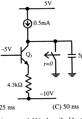
For the BJT $Q_1$ in the circuit shown below, $\beta = \infty$, $V_{BEon} = 0.7\,\text{V}$, $V_{CEsat} = 0.7\,\text{V}$. The switch is initially closed. At time $t=0$, the switch is opened. The time $t$ at which $Q_1$ leaves the active region is
2011 · Electronics & Communication Engineering · Analog Circuits · BJT and MOSFET Amplifiers
Electronics & Communication Engineering (EC) 2011
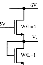
In the circuit shown below, for the MOS transistors, $\mu_n C_{ox} = 100\,\mu\text{A/V}^2$ and the threshold voltage $V_T = 1\,\text{V}$. The voltage $V_x$ at the source of the upper transistor is
2011 · Electronics & Communication Engineering · Analog Circuits · BJT and MOSFET Amplifiers
Electronics & Communication Engineering (EC) 2011
For a BJT, the common-base current gain $\alpha = 0.98$ and the collector base junction reverse bias saturation current $I_{CO} = 0.6\,\mu\text{A}$. This BJT is connected in the common emitter mode and operated in the active region with a base drive current $I_B = 20\,\mu\text{A}$. The collector current $I_C$ for this mode of operation is
2012 · Electronics & Communication Engineering · Analog Circuits · BJT and MOSFET Amplifiers
Electronics & Communication Engineering (EC) 2012
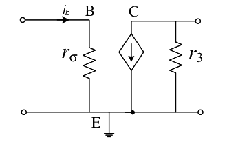
The current \(i_b\) through the base of a silicon \(npn\) transistor is \(1+0.1\cos(10000\pi t)\) mA. At 300 K, the \(r_\pi\) in the small signal model of the transistor is