My Cart
Your Cart 0

    Your cart is empty.

  • Total (Amount) ₹0.00
Previous year question hub

Combinational Logic and Boolean Minimization - Digital Circuits - Electronics & Communication Engineering Previous Year Questions

Practice Combinational Logic and Boolean Minimization - Digital Circuits - Electronics & Communication Engineering previous year questions organised from real papers, with year-wise coverage and clear topic navigation.

21Papers
13Years
63Questions
1Topics

Combinational Logic and Boolean Minimization question pattern

Every graph below is calculated only from this selection.

Questions by year

Year-wise coverage for Combinational Logic and Boolean Minimization. Each bar uses a separate theme-derived color.

Difficulty distribution

How the classified questions are distributed by difficulty.

Medium 37 58.7%
Easy 23 36.5%
Hard 3 4.8%

Question type distribution

MCQ, numerical, multiple-select and other formats found in these papers.

MCQ 50 79.4%
MSQ 6 9.5%
Numerical Answer Type (NAT) 6 9.5%
Fill in the blanks 1 1.6%

Subject weightage

Top subjects by unique question coverage.

Electronics & Communication Engineering
63 Qs

Most asked topics

Top topics across the included previous year papers.

Digital Circuits
63 Qs

Subtopic coverage

Top subtopics inside this exact selection.

Combinational Logic and Boolean Minimization
63 Qs

Paper coverage

Question coverage for the most populated papers. Every active PYP paper remains listed below.

Electronics and Communication Engineering (EC) 2026
3 Qs
Electronics & Communication Engineering (EC) 2025
2 Qs
Electronics & Communication Engineering (EC) 2024
4 Qs
Electronics & Communication Engineering (EC) 2023
2 Qs
Electronics & Communication Engineering (EC) 2022
4 Qs
Electronics & Communication Engineering (EC) 2021
2 Qs
Electronics & Communication Engineering (EC) 2019
5 Qs
Electronics & Communication Engineering (EC) 2018
5 Qs
Electronics & Communication Engineering (EC) 2017
4 Qs
Electronics & Communication Engineering (EC) 2016 [Session 3]
4 Qs
Electronics & Communication Engineering (EC) 2016 [Session 1]
3 Qs
Electronics & Communication Engineering (EC) 2016 [Session 2]
3 Qs
Electronics & Communication Engineering (EC) 2014 [Session 1]
4 Qs
Electronics & Communication Engineering (EC) 2014 [Session 4]
4 Qs
Electronics & Communication Engineering (EC) 2014 [Session 2]
2 Qs
Electronics & Communication Engineering (EC) 2014 [Session 3]
2 Qs
Electronics & Communication Engineering (EC) 2013 [Session 2]
2 Qs
Electronics & Communication Engineering (EC) 2013 [Session 3]
2 Qs
Electronics & Communication Engineering (EC) 2013 [Session 4]
2 Qs
Electronics & Communication Engineering (EC) 2013 [Session 1]
1 Qs
Electronics & Communication Engineering (EC) 2012
3 Qs

Included previous year papers

Newest papers appear first. Sort by year, question coverage or name.

PaperYear / sessionQuestions in this viewOpen
Electronics and Communication Engineering (EC) 202620263View paper
Electronics & Communication Engineering (EC) 202520252View paper
Electronics & Communication Engineering (EC) 202420244View paper
Electronics & Communication Engineering (EC) 202320232View paper
Electronics & Communication Engineering (EC) 202220224View paper
Electronics & Communication Engineering (EC) 202120212View paper
Electronics & Communication Engineering (EC) 201920195View paper
Electronics & Communication Engineering (EC) 201820185View paper
Electronics & Communication Engineering (EC) 201720174View paper
Electronics & Communication Engineering (EC) 2016 [Session 1]20163View paper
Electronics & Communication Engineering (EC) 2016 [Session 2]20163View paper
Electronics & Communication Engineering (EC) 2016 [Session 3]20164View paper
Electronics & Communication Engineering (EC) 2014 [Session 1]20144View paper
Electronics & Communication Engineering (EC) 2014 [Session 2]20142View paper
Electronics & Communication Engineering (EC) 2014 [Session 3]20142View paper
Electronics & Communication Engineering (EC) 2014 [Session 4]20144View paper
Electronics & Communication Engineering (EC) 2013 [Session 1]20131View paper
Electronics & Communication Engineering (EC) 2013 [Session 2]20132View paper
Electronics & Communication Engineering (EC) 2013 [Session 3]20132View paper
Electronics & Communication Engineering (EC) 2013 [Session 4]20132View paper
Electronics & Communication Engineering (EC) 201220123View paper

All Combinational Logic and Boolean Minimization previous year questions

Practice every matching question in batches of 20, with every available option.

1
2012 · Electronics & Communication Engineering · Digital Circuits · Combinational Logic and Boolean Minimization
Electronics & Communication Engineering (EC) 2012

The output Y of a 2-bit comparator is logic 1 whenever the 2-bit input A is greater than the 2-bit input B. The number of combinations for which the output is logic 1, is

Open complete paper
2
2012 · Electronics & Communication Engineering · Digital Circuits · Combinational Logic and Boolean Minimization
Electronics & Communication Engineering (EC) 2012

In the circuit shown

Question diagram

Open complete paper
3
2012 · Electronics & Communication Engineering · Digital Circuits · Combinational Logic and Boolean Minimization
Electronics & Communication Engineering (EC) 2012
In the sum of products function \( f(X, Y, Z) = \sum(2, 3, 4, 5) \), the prime implicants are
Open complete paper
4
2013 · Electronics & Communication Engineering · Digital Circuits · Combinational Logic and Boolean Minimization
Electronics & Communication Engineering (EC) 2013 [Session 1]
A bulb in a staircase has two switches, one switch being at the ground floor and the other one at the first floor. The bulb can be turned ON and also can be turned OFF by any one of the switches irrespective of the state of the other switch. The logic of switching of the bulb resembles
Open complete paper
5
2013 · Electronics & Communication Engineering · Digital Circuits · Combinational Logic and Boolean Minimization
Electronics & Communication Engineering (EC) 2013 [Session 2]
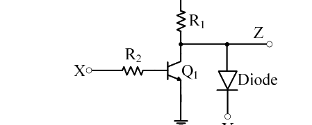
In the circuit shown below, \(Q_1\) has negligible collector-to-emitter saturation voltage and the diode drops negligible voltage across it under forward bias. If \(V_{cc}\) is \(+5\text{ V}\), X and Y are digital signals with 0 V as logic 0 and \(V_{cc}\) as logic 1, then the Boolean expression for Z is
Open complete paper
6
2013 · Electronics & Communication Engineering · Digital Circuits · Combinational Logic and Boolean Minimization
Electronics & Communication Engineering (EC) 2013 [Session 3]
In the circuit shown below, Q1 has negligible collector-to-emitter saturation voltage and the diode drops negligible voltage across it under forward bias. If Vcc is +5 V, X and Y are digital signals with 0 V as logic 0 and Vcc as logic 1, then the Boolean expression for Z is

Question diagram

Open complete paper
7
2014 · Electronics & Communication Engineering · Digital Circuits · Combinational Logic and Boolean Minimization
Electronics & Communication Engineering (EC) 2014 [Session 1]
In the following circuit employing pass transistor logic, all NMOS transistors are identical with a threshold voltage of 1 V. Ignoring the body-effect, the output voltages at P, Q and R are,

Question diagram

Open complete paper
8
2014 · Electronics & Communication Engineering · Digital Circuits · Combinational Logic and Boolean Minimization
Electronics & Communication Engineering (EC) 2014 [Session 1]
The Boolean expression (X + Y)(X + Y̅) + (X̅Y) + X̅ simplifies to
Open complete paper
9
2014 · Electronics & Communication Engineering · Digital Circuits · Combinational Logic and Boolean Minimization
Electronics & Communication Engineering (EC) 2014 [Session 1]
The output $F$ in the digital logic circuit shown in the figure is
Open complete paper
10
2014 · Electronics & Communication Engineering · Digital Circuits · Combinational Logic and Boolean Minimization
Electronics & Communication Engineering (EC) 2014 [Session 1]
Consider the Boolean function, $F(w,x,y,z) = wy + xy + \bar{w}\bar{x}\bar{y}z + \bar{w}\bar{x}y + xz + \bar{x}\bar{y}\bar{z}$. Which one of the following is the complete set of essential prime implicants?
Open complete paper
11
2014 · Electronics & Communication Engineering · Digital Circuits · Combinational Logic and Boolean Minimization
Electronics & Communication Engineering (EC) 2014 [Session 2]
For an n-variable Boolean function, the maximum number of prime implicants is
Open complete paper
12
2014 · Electronics & Communication Engineering · Digital Circuits · Combinational Logic and Boolean Minimization
Electronics & Communication Engineering (EC) 2014 [Session 2]
In a half-subtractor circuit with X and Y as inputs, the Borrow (M) and Difference (N = X - Y) are given by
Open complete paper
13
2014 · Electronics & Communication Engineering · Digital Circuits · Combinational Logic and Boolean Minimization
Electronics & Communication Engineering (EC) 2014 [Session 3]
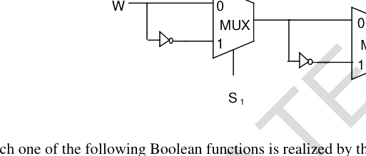
Consider the multiplexer based logic circuit shown in the figure. Which one of the following Boolean functions is realized by the circuit?

Question diagram

Open complete paper
14
2014 · Electronics & Communication Engineering · Digital Circuits · Combinational Logic and Boolean Minimization
Electronics & Communication Engineering (EC) 2014 [Session 3]
In the circuit shown, \(W\) and \(Y\) are MSBs of the control inputs. The output \(F\) is given by

Question diagram

Open complete paper
15
2014 · Electronics & Communication Engineering · Digital Circuits · Combinational Logic and Boolean Minimization
Electronics & Communication Engineering (EC) 2014 [Session 4]
In the circuit shown in the figure, if C = 0, the expression for Y is
Open complete paper
16
2014 · Electronics & Communication Engineering · Digital Circuits · Combinational Logic and Boolean Minimization
Electronics & Communication Engineering (EC) 2014 [Session 4]
The output (Y) of the circuit shown in the figure is

Question diagram

Open complete paper
17
2014 · Electronics & Communication Engineering · Digital Circuits · Combinational Logic and Boolean Minimization
Electronics & Communication Engineering (EC) 2014 [Session 4]
An 8-to-1 multiplexer is used to implement a logical function Y as shown in the figure. The output Y is given by

Question diagram

Open complete paper
18
2014 · Electronics & Communication Engineering · Digital Circuits · Combinational Logic and Boolean Minimization
Electronics & Communication Engineering (EC) 2014 [Session 4]
A 16-bit ripple carry adder is realized using 16 identical full adders (FA) as shown in the figure. The carry-propagation delay of each FA is 12 ns and the sum-propagation delay of each FA is 15 ns. The worst case delay (in ns) of this 16-bit adder will be __________.

Question diagram

Open complete paper
19
2016 · Electronics & Communication Engineering · Digital Circuits · Combinational Logic and Boolean Minimization
Electronics & Communication Engineering (EC) 2016 [Session 1]
The output of the combinational circuit given below is

Question diagram

Open complete paper
20
2016 · Electronics & Communication Engineering · Digital Circuits · Combinational Logic and Boolean Minimization
Electronics & Communication Engineering (EC) 2016 [Session 1]
Identify the circuit below.
Open complete paper

Showing 20 of 59 questions