My Cart
Your Cart 0

    Your cart is empty.

  • Total (Amount) ₹0.00
Previous year question hub

Diode Circuits - Analog Circuits - Electronics & Communication Engineering Previous Year Questions

Practice Diode Circuits - Analog Circuits - Electronics & Communication Engineering previous year questions organised from real papers, with year-wise coverage and clear topic navigation.

21Papers
14Years
38Questions
1Topics

Diode Circuits question pattern

Every graph below is calculated only from this selection.

Questions by year

Year-wise coverage for Diode Circuits. Each bar uses a separate theme-derived color.

Difficulty distribution

How the classified questions are distributed by difficulty.

Medium 34 89.5%
Easy 3 7.9%
Hard 1 2.6%

Question type distribution

MCQ, numerical, multiple-select and other formats found in these papers.

MCQ 23 60.5%
Numerical Answer Type (NAT) 12 31.6%
MSQ 2 5.3%
Fill in the blanks 1 2.6%

Subject weightage

Top subjects by unique question coverage.

Electronics & Communication Engineering
38 Qs

Most asked topics

Top topics across the included previous year papers.

Analog Circuits
38 Qs

Subtopic coverage

Top subtopics inside this exact selection.

Diode Circuits
38 Qs

Paper coverage

Question coverage for the most populated papers. Every active PYP paper remains listed below.

Electronics and Communication Engineering (EC) 2026
1 Qs
Electronics & Communication Engineering (EC) 2025
2 Qs
Electronics & Communication Engineering (EC) 2024
2 Qs
Electronics & Communication Engineering (EC) 2023
1 Qs
Electronics & Communication Engineering (EC) 2022
1 Qs
Electronics & Communication Engineering (EC) 2021
1 Qs
Electronics & Communication Engineering (EC) 2020
1 Qs
Electronics & Communication Engineering (EC) 2019
5 Qs
Electronics & Communication Engineering (EC) 2018
1 Qs
Electronics & Communication Engineering (EC) 2017
2 Qs
Electronics & Communication Engineering (EC) 2016 [Session 2]
3 Qs
Electronics & Communication Engineering (EC) 2016 [Session 3]
2 Qs
Electronics & Communication Engineering (EC) 2016 [Session 1]
1 Qs
Electronics & Communication Engineering (EC) 2014 [Session 1]
1 Qs
Electronics & Communication Engineering (EC) 2014 [Session 2]
1 Qs
Electronics & Communication Engineering (EC) 2014 [Session 4]
1 Qs
Electronics & Communication Engineering (EC) 2013 [Session 3]
3 Qs
Electronics & Communication Engineering (EC) 2013 [Session 4]
3 Qs
Electronics & Communication Engineering (EC) 2013 [Session 1]
2 Qs
Electronics & Communication Engineering (EC) 2013 [Session 2]
2 Qs
Electronics & Communication Engineering (EC) 2012
2 Qs

Included previous year papers

Newest papers appear first. Sort by year, question coverage or name.

PaperYear / sessionQuestions in this viewOpen
Electronics and Communication Engineering (EC) 202620261View paper
Electronics & Communication Engineering (EC) 202520252View paper
Electronics & Communication Engineering (EC) 202420242View paper
Electronics & Communication Engineering (EC) 202320231View paper
Electronics & Communication Engineering (EC) 202220221View paper
Electronics & Communication Engineering (EC) 202120211View paper
Electronics & Communication Engineering (EC) 202020201View paper
Electronics & Communication Engineering (EC) 201920195View paper
Electronics & Communication Engineering (EC) 201820181View paper
Electronics & Communication Engineering (EC) 201720172View paper
Electronics & Communication Engineering (EC) 2016 [Session 1]20161View paper
Electronics & Communication Engineering (EC) 2016 [Session 2]20163View paper
Electronics & Communication Engineering (EC) 2016 [Session 3]20162View paper
Electronics & Communication Engineering (EC) 2014 [Session 1]20141View paper
Electronics & Communication Engineering (EC) 2014 [Session 2]20141View paper
Electronics & Communication Engineering (EC) 2014 [Session 4]20141View paper
Electronics & Communication Engineering (EC) 2013 [Session 1]20132View paper
Electronics & Communication Engineering (EC) 2013 [Session 2]20132View paper
Electronics & Communication Engineering (EC) 2013 [Session 3]20133View paper
Electronics & Communication Engineering (EC) 2013 [Session 4]20133View paper
Electronics & Communication Engineering (EC) 201220122View paper

All Diode Circuits previous year questions

Practice every matching question in batches of 20, with every available option.

1
2012 · Electronics & Communication Engineering · Analog Circuits · Diode Circuits
Electronics & Communication Engineering (EC) 2012
The i-v characteristics of the diode in the circuit given below are \(i = egin{cases} rac{v - 0.7}{500} ext{ A}, & v \geq 0.7 ext{ V} \ 0 ext{ A}, & v < 0.7 ext{ V} \end{cases}\) The current in the circuit is
Open complete paper
2
2012 · Electronics & Communication Engineering · Analog Circuits · Diode Circuits
Electronics & Communication Engineering (EC) 2012
The diodes and capacitors in the circuit shown are ideal. The voltage \(v(t)\) across the diode D1 is

Question diagram

Open complete paper
3
2013 · Electronics & Communication Engineering · Analog Circuits · Diode Circuits
Electronics & Communication Engineering (EC) 2013 [Session 1]
A voltage 1000 sin \(\omega t\) Volts is applied across YZ. Assuming ideal diodes, the voltage measured across WX in Volts, is

Question diagram

Open complete paper
4
2013 · Electronics & Communication Engineering · Analog Circuits · Diode Circuits
Electronics & Communication Engineering (EC) 2013 [Session 1]
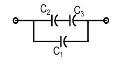
Three capacitors C_1, C_2 and C_3, whose values are 10\(\mu\)F, 5\(\mu\)F, and 2\(\mu\)F respectively, have breakdown voltages of 10V, 5V, and 2V respectively. For the interconnection shown below, the maximum safe voltage in Volts that can be applied across the combination, and the corresponding total charge in \(\mu\)C stored in the effective capacitance across the terminals are respectively,

Question diagram

Open complete paper
5
2013 · Electronics & Communication Engineering · Analog Circuits · Diode Circuits
Electronics & Communication Engineering (EC) 2013 [Session 2]
A voltage \(1000\sin\omega t\) Volts is applied across YZ. Assuming ideal diodes, the voltage measured across WX in Volts, is
Open complete paper
6
2013 · Electronics & Communication Engineering · Analog Circuits · Diode Circuits
Electronics & Communication Engineering (EC) 2013 [Session 2]
In the circuit shown below, the knee current of the ideal Zener diode is 10 mA. To maintain 5 V across \(R_L\), the minimum value of \(R_L\) in \(\Omega\) and the minimum power rating of the Zener diode in mW, respectively, are

Question diagram

Open complete paper
7
2013 · Electronics & Communication Engineering · Analog Circuits · Diode Circuits
Electronics & Communication Engineering (EC) 2013 [Session 3]
Three capacitors C1, C2 and C3, whose values are 10μF, 5μF, and 2μF respectively, have breakdown voltages of 10V, 5V, and 2V respectively. For the interconnection shown below, the maximum safe voltage in Volts that can be applied across the combination, and the corresponding total charge in μC stored in the effective capacitance across the terminals are respectively,

Question diagram

Open complete paper
8
2013 · Electronics & Communication Engineering · Analog Circuits · Diode Circuits
Electronics & Communication Engineering (EC) 2013 [Session 3]
A voltage 1000 sin ωt Volts is applied across YZ. Assuming ideal diodes, the voltage measured across WX in Volts, is

Question diagram

Open complete paper
9
2013 · Electronics & Communication Engineering · Analog Circuits · Diode Circuits
Electronics & Communication Engineering (EC) 2013 [Session 4]
Three capacitors \( C_1 \), \( C_2 \) and \( C_3 \) whose values are 10\(\mu F\), 5\(\mu F\), and 2\(\mu F\) respectively, have breakdown voltages of 10V, 5V, and 2V respectively. For the interconnection shown below, the maximum safe voltage in Volts that can be applied across the combination, and the corresponding total charge in \(\mu C\) stored in the effective capacitance across the terminals are respectively,

Question diagram

Open complete paper
10
2014 · Electronics & Communication Engineering · Analog Circuits · Diode Circuits
Electronics & Communication Engineering (EC) 2014 [Session 1]
In the figure, assume that the forward voltage drops of the PN diode D₁ and Schottky diode D₂ are 0.7 V and 0.3 V, respectively. If ON denotes conducting state of the diode and OFF denotes non-conducting state of the diode, then in the circuit,

Question diagram

Open complete paper
11
2014 · Electronics & Communication Engineering · Analog Circuits · Diode Circuits
Electronics & Communication Engineering (EC) 2014 [Session 2]
The diode in the circuit shown has \( V_{on} = 0.7 \) Volts but is ideal otherwise. If \( V_i = 5 \sin(\omega t) \) Volts, the minimum and maximum values of \( V_o \) (in Volts) are, respectively,
Open complete paper
12
2014 · Electronics & Communication Engineering · Analog Circuits · Diode Circuits
Electronics & Communication Engineering (EC) 2014 [Session 4]
Two silicon diodes, with a forward voltage drop of 0.7 V, are used in the circuit shown in the figure. The range of input voltage \(V_i\) for which the output voltage \(V_o = V_i\), is
Open complete paper
13
2016 · Electronics & Communication Engineering · Analog Circuits · Diode Circuits
Electronics & Communication Engineering (EC) 2016 [Session 1]
An AC voltage source \(V = 10 \sin(t)\) volts is applied to the following network. Assume that \(R_1 = 3 \, \Omega\), \(R_2 = 6 \, \Omega\) and \(R_3 = \, \Omega\), and that the diode is ideal.
RMS current \(I_{rms}\) (in mA) through the diode is ______
Open complete paper
14
2016 · Electronics & Communication Engineering · Analog Circuits · Diode Circuits
Electronics & Communication Engineering (EC) 2016 [Session 2]
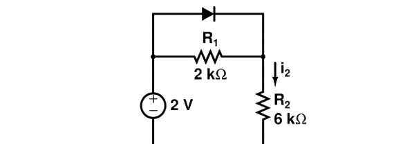
Assume that the diode in the figure has \(V_{on} = 0.7\) V, but is otherwise ideal.

The magnitude of the current \(i_2\) (in mA) is equal to _____

Question diagram

Open complete paper
15
2016 · Electronics & Communication Engineering · Analog Circuits · Diode Circuits
Electronics & Communication Engineering (EC) 2016 [Session 2]
The switch S in the circuit shown has been closed for a long time. It is opened at time $t = 0$ and remains open after that. Assume that the diode has zero reverse current and zero forward voltage drop.
The steady state magnitude of the capacitor voltage $V_C$ (in volts) is ________

Question diagram

Open complete paper
16
2016 · Electronics & Communication Engineering · Analog Circuits · Diode Circuits
Electronics & Communication Engineering (EC) 2016 [Session 2]
The figure shows a half-wave rectifier with a \(475 \ \mu\text{F}\) filter capacitor. The load draws a constant current \(I_O = 1 \text{ A}\) from the rectifier. The figure also shows the input voltage \(V_I\), the output voltage \(V_C\) and the peak-to-peak voltage ripple \(u\) on \(V_C\). The input voltage \(V_I\) is a triangle-wave with an amplitude of \(10 \text{ V}\) and a period of \(1 \text{ ms}\).
The value of the ripple \(u\) (in volts) is ______
Open complete paper
17
2016 · Electronics & Communication Engineering · Analog Circuits · Diode Circuits
Electronics & Communication Engineering (EC) 2016 [Session 3]
The diodes D1 and D2 in the figure are ideal and the capacitors are identical. The product RC is very large compared to the time period of the ac voltage. Assuming that the diodes do not breakdown in the reverse bias, the output voltage VO (in volt) at the steady state is ______
Open complete paper
18
2016 · Electronics & Communication Engineering · Analog Circuits · Diode Circuits
Electronics & Communication Engineering (EC) 2016 [Session 3]
The I-V characteristics of the zener diodes D1 and D2 are shown in Figure I. These diodes are used in the circuit given in Figure II. If the supply voltage is varied from 0 to 100 V, then breakdown occurs in
Open complete paper
19
2017 · Electronics & Communication Engineering · Analog Circuits · Diode Circuits
Electronics & Communication Engineering (EC) 2017
Correct : 1 Wrong : 0

The output Vo of the diode circuit shown in the figure is connected to an averaging DC voltmeter. The reading on the DC voltmeter in Volts, neglecting the voltage drop across the diode, is ________.

Open complete paper
20
2017 · Electronics & Communication Engineering · Analog Circuits · Diode Circuits
Electronics & Communication Engineering (EC) 2017

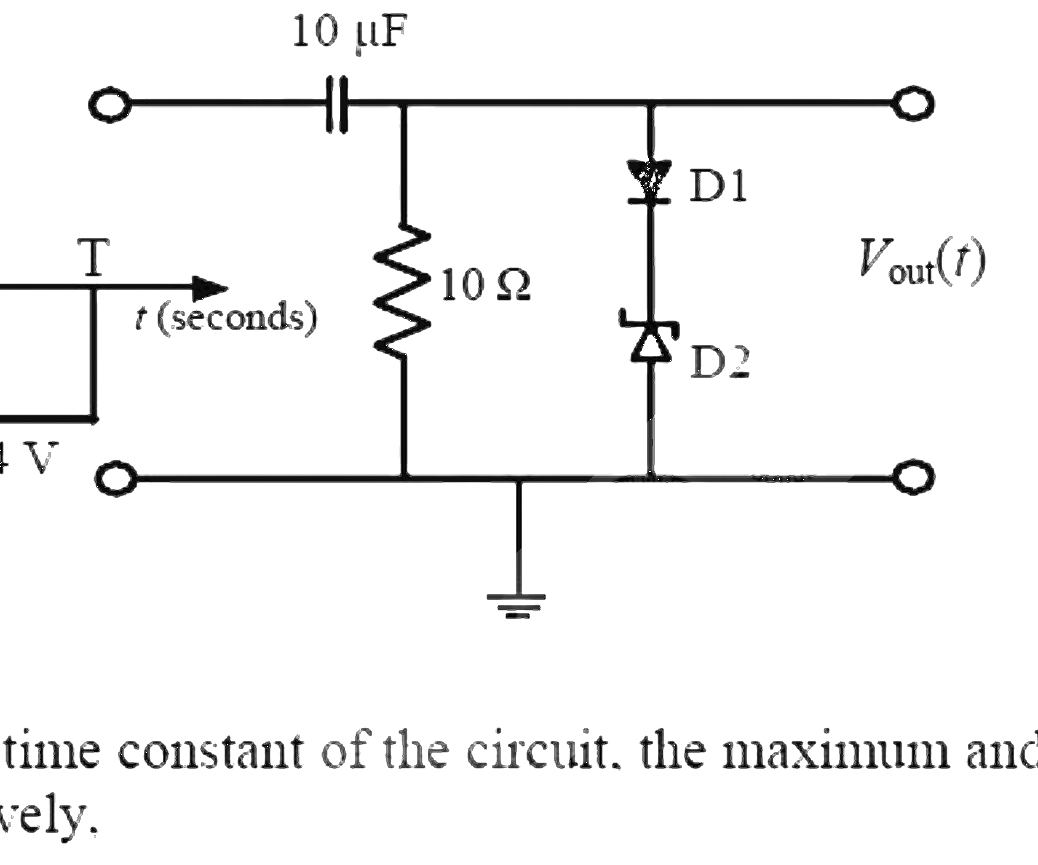
In the figure, D1 is a real silicon pn junction diode with a drop of 0.7 V under forward bias condition and D2 is a Zener diode with breakdown voltage of −6.8 V. The input Vin(t) is a periodic square wave of period T, whose one period is shown in the figure. Assuming 10τ << T, where τ is the time constant of the circuit, the maximum and minimum values of the output waveform are respectively,

Open complete paper

Showing 20 of 35 questions