My Cart
Your Cart 0

    Your cart is empty.

  • Total (Amount) ₹0.00
Previous year question hub

BJT and MOSFET Amplifiers - Analog Circuits - Electronics & Communication Engineering Previous Year Questions

Practice BJT and MOSFET Amplifiers - Analog Circuits - Electronics & Communication Engineering previous year questions organised from real papers, with year-wise coverage and clear topic navigation.

22Papers
14Years
51Questions
1Topics

BJT and MOSFET Amplifiers question pattern

Every graph below is calculated only from this selection.

Questions by year

Year-wise coverage for BJT and MOSFET Amplifiers. Each bar uses a separate theme-derived color.

Difficulty distribution

How the classified questions are distributed by difficulty.

Medium 39 76.5%
Easy 7 13.7%
Hard 5 9.8%
Question type distribution

MCQ, numerical, multiple-select and other formats found in these papers.

MCQ 36 70.6%
Numerical Answer Type (NAT) 10 19.6%
MSQ 3 5.9%
Fill in the blanks 2 3.9%

Subject weightage

Top subjects by unique question coverage.

Electronics & Communication Engineering
51 Qs

Most asked topics

Top topics across the included previous year papers.

Analog Circuits
51 Qs

Subtopic coverage

Top subtopics inside this exact selection.

BJT and MOSFET Amplifiers
51 Qs

Paper coverage

Question coverage for the most populated papers. Every active PYP paper remains listed below.

Electronics and Communication Engineering (EC) 2026
2 Qs
Electronics & Communication Engineering (EC) 2025
5 Qs
Electronics & Communication Engineering (EC) 2024
2 Qs
Electronics & Communication Engineering (EC) 2023
3 Qs
Electronics & Communication Engineering (EC) 2022
3 Qs
Electronics & Communication Engineering (EC) 2021
2 Qs
Electronics & Communication Engineering (EC) 2020
1 Qs
Electronics & Communication Engineering (EC) 2019
2 Qs
Electronics & Communication Engineering (EC) 2018
1 Qs
Electronics & Communication Engineering (EC) 2017
3 Qs
Electronics & Communication Engineering (EC) 2016 [Session 3]
3 Qs
Electronics & Communication Engineering (EC) 2016 [Session 2]
2 Qs
Electronics & Communication Engineering (EC) 2016 [Session 1]
1 Qs
Electronics & Communication Engineering (EC) 2014 [Session 4]
4 Qs
Electronics & Communication Engineering (EC) 2014 [Session 1]
2 Qs
Electronics & Communication Engineering (EC) 2014 [Session 2]
1 Qs
Electronics & Communication Engineering (EC) 2014 [Session 3]
1 Qs
Electronics & Communication Engineering (EC) 2013 [Session 2]
3 Qs
Electronics & Communication Engineering (EC) 2013 [Session 3]
3 Qs
Electronics & Communication Engineering (EC) 2013 [Session 1]
2 Qs
Electronics & Communication Engineering (EC) 2013 [Session 4]
2 Qs
Electronics & Communication Engineering (EC) 2012
3 Qs

Included previous year papers

Newest papers appear first. Sort by year, question coverage or name.

PaperYear / sessionQuestions in this viewOpen
Electronics and Communication Engineering (EC) 202620262View paper
Electronics & Communication Engineering (EC) 202520255View paper
Electronics & Communication Engineering (EC) 202420242View paper
Electronics & Communication Engineering (EC) 202320233View paper
Electronics & Communication Engineering (EC) 202220223View paper
Electronics & Communication Engineering (EC) 202120212View paper
Electronics & Communication Engineering (EC) 202020201View paper
Electronics & Communication Engineering (EC) 201920192View paper
Electronics & Communication Engineering (EC) 201820181View paper
Electronics & Communication Engineering (EC) 201720173View paper
Electronics & Communication Engineering (EC) 2016 [Session 1]20161View paper
Electronics & Communication Engineering (EC) 2016 [Session 2]20162View paper
Electronics & Communication Engineering (EC) 2016 [Session 3]20163View paper
Electronics & Communication Engineering (EC) 2014 [Session 1]20142View paper
Electronics & Communication Engineering (EC) 2014 [Session 2]20141View paper
Electronics & Communication Engineering (EC) 2014 [Session 3]20141View paper
Electronics & Communication Engineering (EC) 2014 [Session 4]20144View paper
Electronics & Communication Engineering (EC) 2013 [Session 1]20132View paper
Electronics & Communication Engineering (EC) 2013 [Session 2]20133View paper
Electronics & Communication Engineering (EC) 2013 [Session 3]20133View paper
Electronics & Communication Engineering (EC) 2013 [Session 4]20132View paper
Electronics & Communication Engineering (EC) 201220123View paper

All BJT and MOSFET Amplifiers previous year questions

Practice every matching question in batches of 20, with every available option.

1
2012 · Electronics & Communication Engineering · Analog Circuits · BJT and MOSFET Amplifiers
Electronics & Communication Engineering (EC) 2012
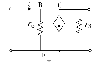
The current \(i_b\) through the base of a silicon \(npn\) transistor is \(1+0.1\cos(10000\pi t)\) mA. At 300 K, the \(r_\pi\) in the small signal model of the transistor is

Question diagram

Open complete paper
2
2012 · Electronics & Communication Engineering · Analog Circuits · BJT and MOSFET Amplifiers
Electronics & Communication Engineering (EC) 2012

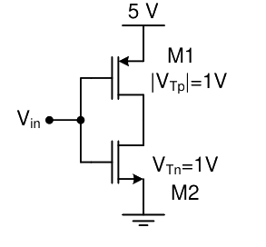
In the CMOS circuit shown, electron and hole mobilities are equal, and M1 and M2 are equally sized. The device M1 is in the linear region if

Question diagram

Open complete paper
3
2012 · Electronics & Communication Engineering · Analog Circuits · BJT and MOSFET Amplifiers
Electronics & Communication Engineering (EC) 2012
The voltage gain \( A_v \) of the circuit shown below is

Question diagram

Open complete paper
4
2013 · Electronics & Communication Engineering · Analog Circuits · BJT and MOSFET Amplifiers
Electronics & Communication Engineering (EC) 2013 [Session 1]
The ac schematic of an NMOS common-source stage is shown in the figure below, where part of the biasing circuits has been omitted for simplicity. For the n-channel MOSFET M, the transconductance gm = 1 mA/V, and body effect and channel length modulation effect are to be neglected. The lower cutoff frequency in Hz of the circuit is approximately at
Open complete paper
5
2013 · Electronics & Communication Engineering · Analog Circuits · BJT and MOSFET Amplifiers
Electronics & Communication Engineering (EC) 2013 [Session 1]
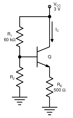
In the circuit shown below, the silicon npn transistor Q has a very high value of \(\beta\). The required value of \(R_2\) in \(k\Omega\) to produce \(I_C = 1\) mA is
Open complete paper
6
2013 · Electronics & Communication Engineering · Analog Circuits · BJT and MOSFET Amplifiers
Electronics & Communication Engineering (EC) 2013 [Session 2]
In the circuit shown below, the silicon npn transistor Q has a very high value of β. The required value of R₂ in kΩ to produce I_C = 1 mA is
Open complete paper
7
2013 · Electronics & Communication Engineering · Analog Circuits · BJT and MOSFET Amplifiers
Electronics & Communication Engineering (EC) 2013 [Session 2]
The small-signal resistance (i.e., \(dV_B/dI_D\)) in \(k\Omega\) offered by the n-channel MOSFET M shown in the figure below, at a bias point of \(V_B = 2 V\) is (device data for M: device transconductance parameter \(k_N = \mu_n C_{ox}(W/L) = 40 \mu A/V^2\), threshold voltage \(V_{TN} = 1 V\), and neglect body effect and channel length modulation effects)

Question diagram

Open complete paper
8
2013 · Electronics & Communication Engineering · Analog Circuits · BJT and MOSFET Amplifiers
Electronics & Communication Engineering (EC) 2013 [Session 2]
The ac schematic of an NMOS common-source stage is shown in the figure below, where part of the biasing circuits has been omitted for simplicity. For the \(n\)-channel MOSFET M, the transconductance \(g_m = 1\) mA/V, and body effect and channel length modulation effect are to be neglected. The lower cutoff frequency in Hz of the circuit is approximately at
Open complete paper
9
2013 · Electronics & Communication Engineering · Analog Circuits · BJT and MOSFET Amplifiers
Electronics & Communication Engineering (EC) 2013 [Session 3]
The ac schematic of an NMOS common-source stage is shown in the figure below, where part of the biasing circuits has been omitted for simplicity. For the \(n\)-channel MOSFET \(M\), the transconductance \(g_m=1\text{ mA/V}\), and body effect and channel length modulation effect are to be neglected. The lower cutoff frequency in Hz of the circuit is approximately at

Question diagram

Open complete paper
10
2013 · Electronics & Communication Engineering · Analog Circuits · BJT and MOSFET Amplifiers
Electronics & Communication Engineering (EC) 2013 [Session 3]
The small-signal resistance (i.e., \(dV_B/dI_D\)) in kΩ offered by the n-channel MOSFET M shown in the figure below, at a bias point of \(V_B=2\text{ V}\) is (device data for M: device transconductance parameter \(k_n=\mu_n C_{ox}^\prime (W/L)=40\text{ μA/V}^2\), threshold voltage \(V_{TN}=1\text{ V}\), and neglect body effect and channel length modulation effects)

Question diagram

Open complete paper
11
2013 · Electronics & Communication Engineering · Analog Circuits · BJT and MOSFET Amplifiers
Electronics & Communication Engineering (EC) 2013 [Session 4]
In the circuit shown below, the silicon npn transistor Q has a very high value of \( \beta \). The required value of \( R_2 \) in k\(\Omega\) to produce \( I_C = 1 \) mA is

Question diagram

Open complete paper
12
2014 · Electronics & Communication Engineering · Analog Circuits · BJT and MOSFET Amplifiers
Electronics & Communication Engineering (EC) 2014 [Session 1]
A good current buffer has
Open complete paper
13
2014 · Electronics & Communication Engineering · Analog Circuits · BJT and MOSFET Amplifiers
Electronics & Communication Engineering (EC) 2014 [Session 1]
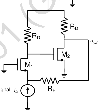
In the ac equivalent circuit shown in the figure, if iin is the input current and RF is very large, the type of feedback is

Question diagram

Open complete paper
14
2014 · Electronics & Communication Engineering · Analog Circuits · BJT and MOSFET Amplifiers
Electronics & Communication Engineering (EC) 2014 [Session 2]
In the differential amplifier shown in the figure, the magnitudes of the common-mode and differential-mode gains are A_cm and A_d, respectively. If the resistance R_E is increased, then

Question diagram

Open complete paper
15
2014 · Electronics & Communication Engineering · Analog Circuits · BJT and MOSFET Amplifiers
Electronics & Communication Engineering (EC) 2014 [Session 3]
In the circuit shown, the silicon BJT has \(\beta = 50\). Assume \(V_{BE} = 0.7\text{ V}\) and \(V_{CE(sat)} = 0.2\text{ V}\). Which one of the following statements is correct?

Question diagram

Open complete paper
16
2014 · Electronics & Communication Engineering · Analog Circuits · BJT and MOSFET Amplifiers
Electronics & Communication Engineering (EC) 2014 [Session 4]
If the emitter resistance in a common-emitter voltage amplifier is not bypassed, it will
Open complete paper
17
2014 · Electronics & Communication Engineering · Analog Circuits · BJT and MOSFET Amplifiers
Electronics & Communication Engineering (EC) 2014 [Session 4]
Consider the common-collector amplifier in the figure (bias circuitry ensures that the transistor operates in forward active region, but has been omitted for simplicity). Let IC be the collector current, VBE be the base-emitter voltage and VT be the thermal voltage. Also, gm and ro are the small-signal transconductance and output resistance of the transistor, respectively. Which one of the following conditions ensures a nearly constant small signal voltage gain for a wide range of values of RE?
Open complete paper
18
2014 · Electronics & Communication Engineering · Analog Circuits · BJT and MOSFET Amplifiers
Electronics & Communication Engineering (EC) 2014 [Session 4]
A BJT in a common-base configuration is used to amplify a signal received by a 50 Ω antenna. Assume kT/q = 25 mV. The value of the collector bias current (in mA) required to match the input impedance of the amplifier to the impedance of the antenna is__________.
Open complete paper
19
2014 · Electronics & Communication Engineering · Analog Circuits · BJT and MOSFET Amplifiers
Electronics & Communication Engineering (EC) 2014 [Session 4]
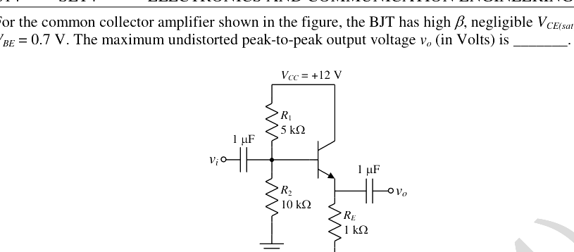
For the common collector amplifier shown in the figure, the BJT has high β, negligible VCE(sat), and VBE = 0.7 V. The maximum undistorted peak-to-peak output voltage vo (in Volts) is __________.

Question diagram

Open complete paper
20
2016 · Electronics & Communication Engineering · Analog Circuits · BJT and MOSFET Amplifiers
Electronics & Communication Engineering (EC) 2016 [Session 1]
What is the voltage \(V_{out}\) in the following circuit?

Question diagram

Open complete paper

Showing 20 of 49 questions