My Cart
Your Cart 0

    Your cart is empty.

  • Total (Amount) ₹0.00
NCERT · Class 12 · Physics

Chapter 14: Semiconductor Electronics: Materials, Devices and Simple Circuits

Practice each question, then open the answer or worked solution.

Questions

15 questions
Q1Multiple choice

In an n-type silicon, which of the following statement is true:

Show solutionHide solution
Worked solution

Here, (c) is the correct option.

For n-type silicon, the majority carriers are electrons, while the minority carriers are holes. An n-type semiconductor is obtained by dropping pentavalent atoms like phosphorus in silicon atoms.

Q2Written answer

Which of the statements given in Exercise 14.1 is true for p-type semiconductors?

Show solutionHide solution
Worked solution

Here, (d) is the correct explanation.

For p-type semiconductor, holes are the majority carriers, while electrons are the minority carriers. A p-type semiconductor is obtained by using trivalent atoms like aluminium in silicon atoms.

Q3Multiple choice

Carbon, silicon and germanium have four valence electrons each. These are characterised by valence and conduction bands separate by energy band gap respectively equal to

\(\begin{array}{l}\left (E_{g} \right )_{Si}\end{array} \)
,
\(\begin{array}{l}\left (E_{g} \right )_{c}\end{array} \)
and
\(\begin{array}{l}\left (E_{g} \right )_{Ge}\end{array} \)
. Which of the following statements is true?

Show answerHide answer
Correct option: C
Show solutionHide solution
Worked solution

(C) is the correct option.

Out of carbon, germanium, and silicon, carbon has the maximum energy bandgap, whereas germanium has the least energy bandgap.

For all these elements, the energy band gap can be related as:

\(\begin{array}{l}\left (E_{g} \right )_{C} > \left (E_{g} \right )_{Si} > \left (E_{g} \right )_{Ge}\end{array} \)
Q4Written answer

In an unbiased p-n junction, holes diffuse to the n-region from the p-region because

(a) free electrons in the n-region attract them.

(b) they move across the junction by the potential difference.

(c) hole concentration in the p-region is more as compared to the n-region.

(d) All of the above.

Show solutionHide solution
Worked solution

(c) is the correct option.

The usual tendency of the charge carriers is to disperse towards the lower concentration region from the higher concentration region. So it can be said that in an unbiased p-n junction, holes disperse from the p-region to the n-region, as the p-region has a greater concentration of holes than in the n-region.

Q5Written answer

When a forward bias is applied to a p-n junction, it

(a) raises the potential barrier.

(b) reduces the majority carrier current to zero.

(c) potential barrier is reduced.

(d) None of the above

Show solutionHide solution
Worked solution

(c) is the correct option

The potential barrier reduces for a p-n junction when a forward bias is applied.

In the above case, the potential barrier across the junction reduces as the applied voltage is opposed by the potential barrier.

Q6Written answer

In half-wave rectification, what is the output frequency if the input frequency is 50 Hz? What is the output frequency of a full-wave rectifier for the same input frequency?

Show solutionHide solution
Worked solution

For a half-wave rectifier, the output frequency is equal to the input frequency. In this case, the input frequency of the half-wave rectifier is 50 Hz.

On the other hand, the output frequency for a full-wave rectifier is twice the input frequency.
Therefore, the output frequency is 2 × 50 = 100 Hz.

Q7Written answer

A p-n photodiode is fabricated from a semiconductor with a bandgap of 2.8 eV. Can it detect a wavelength of 6000 nm?

Show solutionHide solution
Worked solution

No, the photodiode cannot detect the wavelength of 6000 nm because of the following reason:

The energy bandgap of the given photodiode, Eg = 2.8 eV

The wavelength is given by λ = 6000 nm = 6000 × 10−9 m

We can find the energy of the signal from the following relation:

E = hc/λ

In the equation, h is Planck’s constant = 6.626 × 10⁻³⁴ J and c is the speed of light = 3 × 10⁸ m/s

Substituting the values in the equation, we get

E = (6.626 x 10-34 x 3 x 108) / 6000 x 10-9 = 3.313 x 10⁻²⁰ J

But, 1.6 × 10 −19 J = 1 eV

Therefore, E = 3.313 × 10⁻²⁰ J = 3.313 x 10⁻²⁰ / 1.6 x 10-19 = 0.207 eV

The energy of a signal of wavelength 6000 nm is 0.207 eV, which is less than 2.8 eV − the energy band gap of a photodiode. Hence, the photodiode cannot detect the signal.

Q8Written answer

The number of silicon atoms per m3 is 5 × 1028. This is doped simultaneously with 5 × 10²² atoms per m3 of Arsenic and 5 × 10²⁰ per m3 atoms of Indium. Calculate the number of electrons and holes. Given that nI = 1.5 × 10¹⁶m–3. Is the material n-type or p-type?

Show solutionHide solution
Worked solution

The following values are given in the question:

Number of silicon atoms, N = 5 × 10 28 atoms/m3

Number of arsenic atoms, nAS =5×10²²atoms/m3

Number of indium atoms, nIn=5×10²²atoms/m3

ni=1.5×10¹⁶electrons/m3

ne=5×10²²−1.5×1016=4.99×10²²

Let us consider the number of holes to be nh

In the thermal equilibrium, nenh = ni2

Calculating, we get

nh=4.51×10⁹

Here, ne>nh, therefore, the material is an n-type semiconductor.

Q 9: In an intrinsic semiconductor, the energy gap Eg is 1.2eV. Its hole mobility is much smaller than electron mobility and independent of temperature. What is the ratio between conductivity at 600K and that at 300K? Assume that the temperature dependence of intrinsic carrier concentration ni is given by

\(\begin{array}{l}n_{i}=n_{0}exp\left [ -\frac{E_{g}}{2k_{B}T} \right ]\end{array} \)

where n0 is constant.

Energy gap in an intrinsic semiconductor, Eg = 1.2 eV

The temperature dependence of the intrinsic carrier concentration is given as

\(\begin{array}{l}n_{i}=n_{0}exp\left [ -\frac{E_{g}}{2k_{B}T} \right ]\end{array} \)

Here, kB is the Boltzmann constant = 8.62 x 10⁻⁵ eV/K

T is the temperature

n0 is a constant

Initial temperature, T1 = 300 K

The intrinsic carrier concentration at the temperature 300 K can be written as

\(\begin{array}{l}n_{i1}=n_{0}exp\left [ -\frac{E_{g}}{2k_{B}\times 300} \right ]\end{array} \)

Final temperature, T2 = 600 K

The intrinsic carrier concentration at the temperature 600 K can be written as

\(\begin{array}{l}n_{i2}=n_{0}exp\left [ -\frac{E_{g}}{2k_{B}\times 600} \right ]\end{array} \)

The ratio between conductivity at 600K and that at 300K is equal to the ratio between the respective carrier concentration at these temperatures.

\(\begin{array}{l}\frac{n_{i2}}{n_{i1}}= \frac{n_{0}exp\left [ -\frac{E_{g}}{2k_{B}\times 600} \right ]}{n_{0}exp\left [ -\frac{E_{g}}{2k_{B}\times 300} \right ]}\end{array} \)


\(\begin{array}{l}= exp \frac{E_{g}}{2k_{B}}\left [ \frac{1}{300}-\frac{1}{600} \right ]\end{array} \)


\(\begin{array}{l}= exp \frac{1.2}{2\times 8.62\times 10^{-5}}\left [ \frac{1}{300}-\frac{1}{600} \right ]\end{array} \)


\(\begin{array}{l}= exp \frac{1.2}{17.24\times 10^{-5}}\left [ \frac{2-1}{600} \right ]\end{array} \)

= exp (11.6) = 1.09 x 10⁵

There, the ratio between the conductivities is 1.09 x 10⁵.
Q9Written answer

In an intrinsic semiconductor, the energy gap Eg is 1.2eV. Its hole mobility is much smaller than electron mobility and independent of temperature. What is the ratio between conductivity at 600K and that at 300K? Assume that the temperature dependence of intrinsic carrier concentration ni is given by

\(\begin{array}{l}n_{i}=n_{0}exp\left [ -\frac{E_{g}}{2k_{B}T} \right ]\end{array} \)

where n0 is constant.

Show solutionHide solution
Worked solution

Energy gap in an intrinsic semiconductor, Eg = 1.2 eV

The temperature dependence of the intrinsic carrier concentration is given as

\(\begin{array}{l}n_{i}=n_{0}exp\left [ -\frac{E_{g}}{2k_{B}T} \right ]\end{array} \)

Here, kB is the Boltzmann constant = 8.62 x 10⁻⁵ eV/K

T is the temperature

n0 is a constant

Initial temperature, T1 = 300 K

The intrinsic carrier concentration at the temperature 300 K can be written as

\(\begin{array}{l}n_{i1}=n_{0}exp\left [ -\frac{E_{g}}{2k_{B}\times 300} \right ]\end{array} \)

Final temperature, T2 = 600 K

The intrinsic carrier concentration at the temperature 600 K can be written as

\(\begin{array}{l}n_{i2}=n_{0}exp\left [ -\frac{E_{g}}{2k_{B}\times 600} \right ]\end{array} \)

The ratio between conductivity at 600K and that at 300K is equal to the ratio between the respective carrier concentration at these temperatures.

\(\begin{array}{l}\frac{n_{i2}}{n_{i1}}= \frac{n_{0}exp\left [ -\frac{E_{g}}{2k_{B}\times 600} \right ]}{n_{0}exp\left [ -\frac{E_{g}}{2k_{B}\times 300} \right ]}\end{array} \)


\(\begin{array}{l}= exp \frac{E_{g}}{2k_{B}}\left [ \frac{1}{300}-\frac{1}{600} \right ]\end{array} \)


\(\begin{array}{l}= exp \frac{1.2}{2\times 8.62\times 10^{-5}}\left [ \frac{1}{300}-\frac{1}{600} \right ]\end{array} \)


\(\begin{array}{l}= exp \frac{1.2}{17.24\times 10^{-5}}\left [ \frac{2-1}{600} \right ]\end{array} \)

= exp (11.6) = 1.09 x 10⁵

There, the ratio between the conductivities is 1.09 x 10⁵.
Q10Written answer

In a p-n junction diode, the current I can be expressed as

\(\begin{array}{l}I = I_{0}exp\left ( \frac{eV}{2k_{B}T}-1\right )\end{array} \)

where I0 is called the reverse saturation current, V is the voltage across the diode and is positive for forward bias and negative for reverse bias, and I is the current through the diode, kB is the Boltzmann constant (8.6×10⁻⁵ eV/K), and T is the absolute temperature. If for a given diode I0 = 5 × 10–12 A and T = 300 K, then
(a) What will be the forward current at a forward voltage of 0.6 V?
(b) What will be the increase in the current if the voltage across the diode is increased to 0.7 V?
(c) What is the dynamic resistance?
(d) What will be the current if reverse bias voltage changes from 1 V to 2 V?

​Ans:

In a p-n junction diode, the expression for current is given as

\(\begin{array}{l}I = I_{0}exp\left ( \frac{eV}{2k_{B}T}-1\right )\end{array} \)

Here, I0 = 5 × 10–12 A

T = 300 K

kB is the Boltzmann constant = 8.6 x 10⁻⁵ eV/k =  8.6 x 10-5 x 1.6 x 10-19 = 1.376 x 10⁻²³ J/K

(a) Forward voltage, V = 0.6 V

\(\begin{array}{l}I = 5\times 10^{-12}exp\left ( \frac{1.6\times 10^{-19}\times 0.6}{2\times 1.376\times 10^{-23}\times 300}-1\right )\end{array} \)


\(\begin{array}{l}I = 5\times 10^{-12}exp (22.36)\end{array} \)

= 0.0256 A

(b) Voltage across the diode is increased to 0.7 V

\(\begin{array}{l}I’ = 5\times 10^{-12}exp\left ( \frac{1.6\times 10^{-19}\times 0.7}{2\times 1.376\times 10^{-23}\times 300}-1\right )\end{array} \)


\(\begin{array}{l}I’ = 5\times 10^{-12}exp (26.25)\end{array} \)

I’ = 1.257 A

Change in current, ΔI = I’ – I

= 1.257 – 0.0256

= 1.23 A

Change is voltage = 0.7 – 0.6 = 0.1 V

(c) Dynamic resistance = Change in voltage/ Change in current

= 0.1/1.23

= 0.081 Ω

(d) If the reverse bias voltage changes from 1 V to 2 V, the current will almost remain equal to I0 in both cases. Therefore, the dynamic resistance in the reverse bias will be infinite.

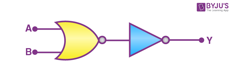
Q 11. You are given the two circuits as shown in Fig. 14.36. Show that
circuit (a) acts as OR gate while circuit (b) acts as AND gate.

a)
NCERT Solutions for Class 12 Physics Chapter 14 Semiconductor Electronics Materials Question 11 Image 1
b)

Show solutionHide solution
Worked solution

(a) Input for the circuit: A and B

Output for the circuit: Y

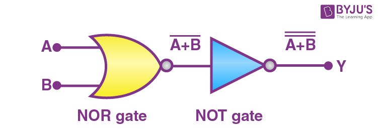
Here, the left half of the circuit works as the NOR gate, while if we look at the right half of the circuit, then it is a NOT gate.

We can show it in the figure as:

NCERT Solutions for Class 12 Physics Chapter 14 Semiconductor Electronics Materials Question 11 Solution Image 1

Now, the output for the NOR gate =

\(\begin{array}{l}\overline{A + B}\end{array} \)

We are giving the output from NOR gate to the input at the NOT gate. So, its output will be

\(\begin{array}{l}\overline{\overline{A + B}}\end{array} \)
\(\begin{array}{l}∴ Y = A + B\end{array} \)

Hence, this circuit functions as an OR Gate.

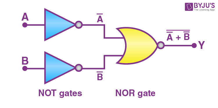
(b) Input for the circuit: A and B

Output for the circuit: Y

We can observe from the figure that the output from the first half of the circuits goes to the input of the next half, which is working as NOR gate.

NCERT Solutions for Class 12 Physics Chapter 14 Semiconductor Electronics Materials Question 11 Solution Image 2

Hence, the output of the given circuit can be written as

\(\begin{array}{l}Y = \overline{\bar{A} + \bar{B}} = \bar{\bar{A}}.\bar{\bar{B}} = A.B\end{array} \)

Hence, this circuit functions as an AND gate.