My Cart
Your Cart 0

    Your cart is empty.

  • Total (Amount) ₹0.00
Previous year question hub

Electronic Properties - Properties and Applications of Materials - Engineering Sciences Previous Year Questions

Practice Electronic Properties - Properties and Applications of Materials - Engineering Sciences previous year questions organised from real papers, with year-wise coverage and clear topic navigation.

15Papers
15Years
38Questions
1Topics

Electronic Properties question pattern

Every graph below is calculated only from this selection.

Questions by year

Year-wise coverage for Electronic Properties. Each bar uses a separate theme-derived color.

Difficulty distribution

How the classified questions are distributed by difficulty.

Easy 25 65.8%
Medium 13 34.2%

Question type distribution

MCQ, numerical, multiple-select and other formats found in these papers.

MCQ 18 47.4%
Numerical Answer Type (NAT) 17 44.7%
MSQ 3 7.9%

Subject weightage

Top subjects by unique question coverage.

Engineering Sciences
38 Qs

Most asked topics

Top topics across the included previous year papers.

Properties and Applications of Materials
38 Qs

Subtopic coverage

Top subtopics inside this exact selection.

Electronic Properties
38 Qs

Paper coverage

Question coverage for the most populated papers. Every active PYP paper remains listed below.

Engineering Sciences (XE) 2026
4 Qs
Engineering Sciences (XE) 2025
3 Qs
Engineering Sciences (XE) 2024
3 Qs
Engineering Sciences (XE) 2023
2 Qs
Engineering Sciences (XE) 2022
2 Qs
Engineering Sciences (XE) 2021
2 Qs
Engineering Sciences (XE) 2020
4 Qs
Engineering Sciences (XE) 2019
2 Qs
Engineering Sciences (XE) 2018
2 Qs
Engineering Sciences (XE) 2017
3 Qs
Engineering Sciences (XE) 2016
2 Qs
Engineering Sciences (XE) 2015
4 Qs
Engineering Sciences (XE) 2014
3 Qs
Engineering Sciences (XE) 2012
1 Qs
Engineering Sciences (XE) 2010
1 Qs

Included previous year papers

Newest papers appear first. Sort by year, question coverage or name.

PaperYear / sessionQuestions in this viewOpen
Engineering Sciences (XE) 202620264View paper
Engineering Sciences (XE) 202520253View paper
Engineering Sciences (XE) 202420243View paper
Engineering Sciences (XE) 202320232View paper
Engineering Sciences (XE) 202220222View paper
Engineering Sciences (XE) 202120212View paper
Engineering Sciences (XE) 202020204View paper
Engineering Sciences (XE) 201920192View paper
Engineering Sciences (XE) 201820182View paper
Engineering Sciences (XE) 201720173View paper
Engineering Sciences (XE) 201620162View paper
Engineering Sciences (XE) 201520154View paper
Engineering Sciences (XE) 201420143View paper
Engineering Sciences (XE) 201220121View paper
Engineering Sciences (XE) 201020101View paper

All Electronic Properties previous year questions

Practice every matching question in batches of 20, with every available option.

1
2010 · Engineering Sciences · Properties and Applications of Materials · Electronic Properties
Engineering Sciences (XE) 2010
The density of states (DOS), for 1 cm3 of Cu, at Fermi level per meV is
Open complete paper
2
2012 · Engineering Sciences · Properties and Applications of Materials · Electronic Properties
Engineering Sciences (XE) 2012
The electron concentration in an n-type semiconductor is 5 × 10¹⁸/m3. If the drift velocity of electrons is 100 m/s in an electric field of 500 V/m, calculate the conductivity of the semiconductor.
Open complete paper
3
2014 · Engineering Sciences · Properties and Applications of Materials · Electronic Properties
Engineering Sciences (XE) 2014
At room temperature, the typical barrier potential for silicon p-n junction in Volt (V) is
Open complete paper
4
2014 · Engineering Sciences · Properties and Applications of Materials · Electronic Properties
Engineering Sciences (XE) 2014
At low injection level, a forward biased p-n junction would have
Open complete paper
5
2014 · Engineering Sciences · Properties and Applications of Materials · Electronic Properties
Engineering Sciences (XE) 2014
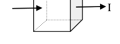
The volume resistivity of a polymeric material is 10¹⁷ Ωm. Find the resistance (in MΩ) of a cube of the material of side 1 cm. The direction of current flow is as shown in the figure below.

Question diagram

Open complete paper
6
2015 · Engineering Sciences · Properties and Applications of Materials · Electronic Properties
Engineering Sciences (XE) 2015

What would be the maximum number of electron-hole pairs that can be generated using a silicon detector irradiated by x-ray of energy 1.54 keV. The band gap of silicon is 1.1 eV.

Question diagram

Open complete paper
7
2015 · Engineering Sciences · Properties and Applications of Materials · Electronic Properties
Engineering Sciences (XE) 2015
The slope of a graph of loge(conductivity) versus 1/T (where T is the temperature) for an intrinsic semiconductor with energy gap Eg is
Open complete paper
8
2015 · Engineering Sciences · Properties and Applications of Materials · Electronic Properties
Engineering Sciences (XE) 2015
A capacitor has a 0.075 cm thick BaTiO₃ dielectric with a dielectric constant of 2000 and an electrode area of 0.2 cm². What is the capacitance of this capacitor in nF?
Open complete paper
9
2015 · Engineering Sciences · Properties and Applications of Materials · Electronic Properties
Engineering Sciences (XE) 2015
The correct statement with regard to electrical property of polymeric materials is
Open complete paper
10
2016 · Engineering Sciences · Properties and Applications of Materials · Electronic Properties
Engineering Sciences (XE) 2016
For a typical metal at room temperature and atmospheric pressure, the Fermi energy is defined as the energy level for which the probability of occupancy is:
Open complete paper
11
2016 · Engineering Sciences · Properties and Applications of Materials · Electronic Properties
Engineering Sciences (XE) 2016
In the photoelectric effect, electrons are ejected
Open complete paper
12
2017 · Engineering Sciences · Properties and Applications of Materials · Electronic Properties
Engineering Sciences (XE) 2017
Which of the following statement(s) is/are true
(i) All piezoelectric materials are necessarily ferroelectric
(ii) All ferroelectric materials are necessarily piezoelectric
(iii) All pyroelectric materials are necessarily piezoelectric
(iv) All pyroelectric materials are necessarily ferroelectric
Open complete paper
13
2017 · Engineering Sciences · Properties and Applications of Materials · Electronic Properties
Engineering Sciences (XE) 2017
Which of the following treatment(s) can increase the electrical conductivity of silicon (i) Heating (ii) Doping with arsenic (iii) Doping with aluminium (iv) Exposure to light
Open complete paper
14
2017 · Engineering Sciences · Properties and Applications of Materials · Electronic Properties
Engineering Sciences (XE) 2017
Copper is an FCC metal with lattice parameter of 3.62 Å. Hall effect measurement shows electron mobility to be 3.2×10³ m2V-1s-1. Electrical resistivity of copper is 1.7 x10⁻⁸ Ωm. The average number of free electrons per atom in copper is ……………….(Charge of an electron: 1.6x10⁻¹⁹ C)
Open complete paper
15
2018 · Engineering Sciences · Properties and Applications of Materials · Electronic Properties
Engineering Sciences (XE) 2018
An electron makes a transition from the valence band to the conduction band in an indirect band gap semiconductor. Which one of the following is true?
Open complete paper
16
2018 · Engineering Sciences · Properties and Applications of Materials · Electronic Properties
Engineering Sciences (XE) 2018
An intrinsic semiconductor has conduction electron concentration, \( n = 10^{12} \text{ cm}^{-3} \). The mobility of both electrons and holes are identical = \( 4 \times 10^4 \text{ cm}^2 \text{ V}^{-1} \text{ s}^{-1} \). If a voltage of 100 V is applied on two parallel end faces of the cube (edge length 1 cm) through Ohmic contacts, the current through the cube would be (in mA)
(Given: charge of electron = \( 1.6 \times 10^{-19} \) C)
Open complete paper
17
2019 · Engineering Sciences · Properties and Applications of Materials · Electronic Properties
Engineering Sciences (XE) 2019
GaAs has advantage over silicon when used in intergrated circuits at low power because it has
Open complete paper
18
2019 · Engineering Sciences · Properties and Applications of Materials · Electronic Properties
Engineering Sciences (XE) 2019
The de Broglie wavelength of an electron accelerated across a 300 kV potential in an electron microscope is ______ ×10-12 m. Ignore relativistic effects. (round off to 2 decimal places) (Given: Planck’s constant = 6.63×10⁻³⁴ J s, electron rest mass = 9.11×10⁻³¹ kg, electron charge = 1.6×10⁻¹⁹ C)
Open complete paper
19
2020 · Engineering Sciences · Properties and Applications of Materials · Electronic Properties
Engineering Sciences (XE) 2020
Density of states, D(E), in a three dimensional solid varies with energy (E) as
Open complete paper
20
2020 · Engineering Sciences · Properties and Applications of Materials · Electronic Properties
Engineering Sciences (XE) 2020
Pure silicon (Si) has a band gap (Eg) of 1.1 eV. This Si is doped with 1 ppm (parts per million) of phosphorus atoms. Si contains 5 × 1028 atoms per m3 in pure form. At temperature T = 300 K, the shift in Fermi energy upon doping with respect to intrinsic Fermi level of pure Si will be ______ eV (with appropriate sign and round-off to two decimal places).
Intrinsic carrier concentration of Si, ni, is given as:
\( n_i = 2\left(\frac{2\pi m k_B T}{h^2}\right)^{3/2} \exp\left(-\frac{E_g}{2 k_B T}\right) \)
Given:
Mass of an electron, m = 9.1 × 10⁻³¹ kg.
Charge of an electron, e = 1.6 × 10⁻¹⁹ C
Boltzmann constant, kB = 1.38 × 10⁻²³ J.K-1
Planck's constant, h = 6.6 × 10⁻³⁴ J.s-1
Open complete paper

Showing 20 of 38 questions