My Cart
Your Cart 0

    Your cart is empty.

  • Total (Amount) ₹0.00
Previous year question hub

Sequential Circuits - Digital Circuits - Electronics & Communication Engineering Previous Year Questions

Practice Sequential Circuits - Digital Circuits - Electronics & Communication Engineering previous year questions organised from real papers, with year-wise coverage and clear topic navigation.

16Papers
13Years
25Questions
1Topics

Sequential Circuits question pattern

Every graph below is calculated only from this selection.

Questions by year

Year-wise coverage for Sequential Circuits. Each bar uses a separate theme-derived color.

Difficulty distribution

How the classified questions are distributed by difficulty.

Medium 22 88%
Easy 2 8%
Hard 1 4%
Question type distribution

MCQ, numerical, multiple-select and other formats found in these papers.

MCQ 15 60%
Numerical Answer Type (NAT) 9 36%
Fill in the blanks 1 4%

Subject weightage

Top subjects by unique question coverage.

Electronics & Communication Engineering
25 Qs

Most asked topics

Top topics across the included previous year papers.

Digital Circuits
25 Qs

Subtopic coverage

Top subtopics inside this exact selection.

Sequential Circuits
25 Qs

Paper coverage

Question coverage for the most populated papers. Every active PYP paper remains listed below.

Electronics and Communication Engineering (EC) 2026
3 Qs
Electronics & Communication Engineering (EC) 2025
2 Qs
Electronics & Communication Engineering (EC) 2024
1 Qs
Electronics & Communication Engineering (EC) 2023
2 Qs
Electronics & Communication Engineering (EC) 2022
1 Qs
Electronics & Communication Engineering (EC) 2021
1 Qs
Electronics & Communication Engineering (EC) 2020
2 Qs
Electronics & Communication Engineering (EC) 2019
2 Qs
Electronics & Communication Engineering (EC) 2018
2 Qs
Electronics & Communication Engineering (EC) 2017
1 Qs
Electronics & Communication Engineering (EC) 2016 [Session 2]
2 Qs
Electronics & Communication Engineering (EC) 2016 [Session 3]
1 Qs
Electronics & Communication Engineering (EC) 2014 [Session 1]
1 Qs
Electronics & Communication Engineering (EC) 2014 [Session 2]
1 Qs
Electronics & Communication Engineering (EC) 2014 [Session 3]
1 Qs
Electronics & Communication Engineering (EC) 2012
2 Qs

Included previous year papers

Newest papers appear first. Sort by year, question coverage or name.

PaperYear / sessionQuestions in this viewOpen
Electronics and Communication Engineering (EC) 202620263View paper
Electronics & Communication Engineering (EC) 202520252View paper
Electronics & Communication Engineering (EC) 202420241View paper
Electronics & Communication Engineering (EC) 202320232View paper
Electronics & Communication Engineering (EC) 202220221View paper
Electronics & Communication Engineering (EC) 202120211View paper
Electronics & Communication Engineering (EC) 202020202View paper
Electronics & Communication Engineering (EC) 201920192View paper
Electronics & Communication Engineering (EC) 201820182View paper
Electronics & Communication Engineering (EC) 201720171View paper
Electronics & Communication Engineering (EC) 2016 [Session 2]20162View paper
Electronics & Communication Engineering (EC) 2016 [Session 3]20161View paper
Electronics & Communication Engineering (EC) 2014 [Session 1]20141View paper
Electronics & Communication Engineering (EC) 2014 [Session 2]20141View paper
Electronics & Communication Engineering (EC) 2014 [Session 3]20141View paper
Electronics & Communication Engineering (EC) 201220122View paper

All Sequential Circuits previous year questions

Practice every matching question in batches of 20, with every available option.

1
2012 · Electronics & Communication Engineering · Digital Circuits · Sequential Circuits
Electronics & Communication Engineering (EC) 2012
Consider the given circuit. In this circuit, the race around

Question diagram

Open complete paper
2
2012 · Electronics & Communication Engineering · Digital Circuits · Sequential Circuits
Electronics & Communication Engineering (EC) 2012

The state transition diagram for the logic circuit shown is

Question diagram

Open complete paper
3
2014 · Electronics & Communication Engineering · Digital Circuits · Sequential Circuits
Electronics & Communication Engineering (EC) 2014 [Session 1]
The digital logic shown in the figure satisfies the given state diagram when Q1 is connected to input A of the XOR gate. Suppose the XOR gate is replaced by an XNOR gate. Which one of the following options preserves the state diagram?
Open complete paper
4
2014 · Electronics & Communication Engineering · Digital Circuits · Sequential Circuits
Electronics & Communication Engineering (EC) 2014 [Session 2]
The outputs of the two flip-flops Q1, Q2 in the figure shown are initialized to 0, 0. The sequence generated at Q1 upon application of clock signal is

Question diagram

Open complete paper
5
2014 · Electronics & Communication Engineering · Digital Circuits · Sequential Circuits
Electronics & Communication Engineering (EC) 2014 [Session 3]
The circuit shown in the figure is a

Question diagram

Open complete paper
6
2016 · Electronics & Communication Engineering · Digital Circuits · Sequential Circuits
Electronics & Communication Engineering (EC) 2016 [Session 2]
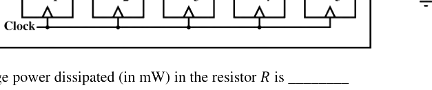
Assume that all the digital gates in the circuit shown in the figure are ideal, the resistor \(R = 10\) k\(\Omega\) and the supply voltage is 5 V. The D flip-flops \(D_1\), \(D_2\), \(D_3\), \(D_4\) and \(D_5\) are initialized with logic values 0,1,0,1 and 0, respectively. The clock has a 30% duty cycle.

The average power dissipated (in mW) in the resistor \(R\) is _____

Question diagram

Open complete paper
7
2016 · Electronics & Communication Engineering · Digital Circuits · Sequential Circuits
Electronics & Communication Engineering (EC) 2016 [Session 2]
The state transition diagram for a finite state machine with states A, B and C, and binary inputs X, Y and Z, is shown in the figure. Which one of the following statements is correct?
Open complete paper
8
2016 · Electronics & Communication Engineering · Digital Circuits · Sequential Circuits
Electronics & Communication Engineering (EC) 2016 [Session 3]
For the circuit shown in the figure, the delay of the bubbled NAND gate is 2 ns and that of the counter is assumed to be zero.

If the clock (Clk) frequency is 1 GHz, then the counter behaves as a
Open complete paper
9
2017 · Electronics & Communication Engineering · Digital Circuits · Sequential Circuits
Electronics & Communication Engineering (EC) 2017

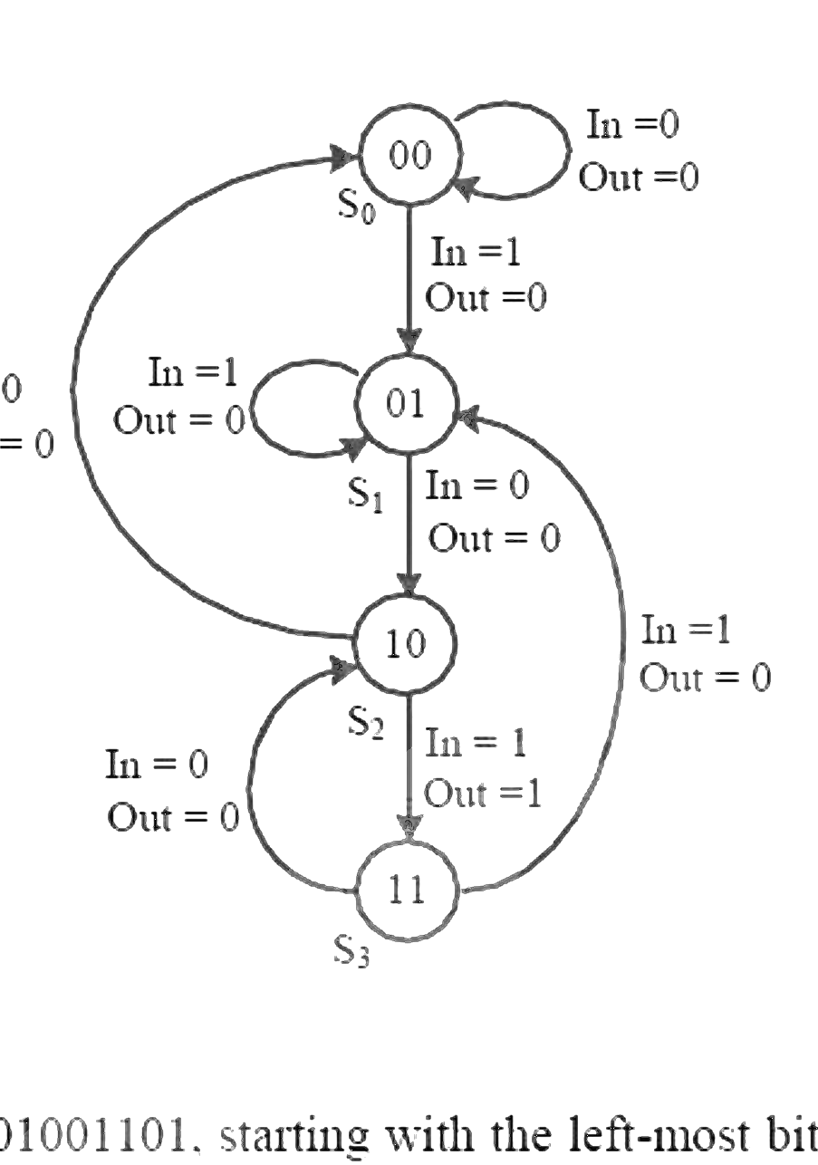
The state diagram of a finite state machine (FSM) designed to detect an overlapping sequence of three bits is shown in the figure. The FSM has an input 'In' and an output 'Out'. The initial state of the FSM is S0. If the input sequence is 10101101001101, starting with the left-most bit, then the number of times 'Out' will be 1 is ________
Open complete paper
10
2018 · Electronics & Communication Engineering · Digital Circuits · Sequential Circuits
Electronics & Communication Engineering (EC) 2018
A traffic signal cycles from GREEN to YELLOW, YELLOW to RED and RED to GREEN. In each cycle, GREEN is turned on for 70 seconds, YELLOW is turned on for 5 seconds and the RED is turned on for 75 seconds. This traffic light has to be implemented using a finite state machine (FSM). The only input to this FSM is a clock of 5 second period. The minimum number of flip-flops required to implement this FSM is ______.
Open complete paper
11
2018 · Electronics & Communication Engineering · Digital Circuits · Sequential Circuits
Electronics & Communication Engineering (EC) 2018
In the circuit shown below, a positive edge-triggered D Flip-Flop is used for sampling input data Din using clock CK. The XOR gate outputs 3.3 volts for logic HIGH and 0 volts for logic LOW levels. The data bit and clock periods are equal and the value of ΔT/TCK = 0.15, where the parameters ΔT and TCK are shown in the figure. Assume that the Flip-Flop and the XOR gate are ideal.
If the probability of input data bit (Din) transition in each clock period is 0.3, the average value (in volts, accurate to two decimal places) of the voltage at node X, is ______.
Open complete paper
12
2019 · Electronics & Communication Engineering · Digital Circuits · Sequential Circuits
Electronics & Communication Engineering (EC) 2019
In the circuit shown, the clock frequency, i.e., the frequency of the Clk signal, is 12 kHz. The frequency of the signal at \( Q_2 \) is ______ kHz.
Open complete paper
13
2019 · Electronics & Communication Engineering · Digital Circuits · Sequential Circuits
Electronics & Communication Engineering (EC) 2019

The state transition diagram for the circuit shown is

Open complete paper
14
2020 · Electronics & Communication Engineering · Digital Circuits · Sequential Circuits
Electronics & Communication Engineering (EC) 2020
The state diagram of a sequence detector is shown below. State S0 is the initial state of the sequence detector. If the output is 1, then
Open complete paper
15
2020 · Electronics & Communication Engineering · Digital Circuits · Sequential Circuits
Electronics & Communication Engineering (EC) 2020
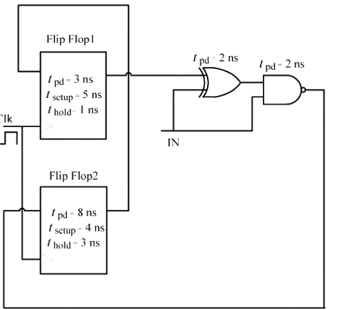
For the components in the sequential circuit shown below, \( t_{pd} \) is the propagation delay, \( t_{setup} \) is the setup time, and \( t_{hold} \) is the hold time. The maximum clock frequency (rounded off to the nearest integer), at which the given circuit can operate reliably, is _____ MHz.

Question diagram

Open complete paper
16
2021 · Electronics & Communication Engineering · Digital Circuits · Sequential Circuits
Electronics & Communication Engineering (EC) 2021
The propagation delay of the exclusive-OR (XOR) gate in the circuit in the figure is 3 ns. The propagation delay of all the flip-flops is assumed to be zero. The clock (Clk) frequency provided to the circuit is 500 MHz.
Starting from the initial value of the flip-flop outputs \(Q_2Q_1Q_0 = 1 1 1\) with \(D_2 = 1\), the minimum number of triggering clock edges after which the flip-flop outputs \(Q_2Q_1Q_0\) becomes 1 0 0 (in integer) is __________.
Open complete paper
17
2022 · Electronics & Communication Engineering · Digital Circuits · Sequential Circuits
Electronics & Communication Engineering (EC) 2022
For the circuit shown, the clock frequency is \(f_0\) and the duty cycle is 25%. For the signal at the Q output of the Flip-Flop, ________.
Open complete paper
18
2023 · Electronics & Communication Engineering · Digital Circuits · Sequential Circuits
Electronics & Communication Engineering (EC) 2023

The synchronous sequential circuit shown below works at a clock frequency of 1 GHz. The throughput, in Mbits/s, and the latency, in ns, respectively, are

Open complete paper
19
2023 · Electronics & Communication Engineering · Digital Circuits · Sequential Circuits
Electronics & Communication Engineering (EC) 2023
In a given sequential circuit, initial states are \(Q_1 = 1\) and \(Q_2 = 0\). For a clock frequency of 1 MHz, the frequency of signal \(Q_2\) in kHz, is ______ (rounded off to the nearest integer).
Open complete paper
20
2024 · Electronics & Communication Engineering · Digital Circuits · Sequential Circuits
Electronics & Communication Engineering (EC) 2024
The sequence of states \( (Q_1 Q_0) \) of the given synchronous sequential circuit is ______.
Open complete paper

Showing 20 of 25 questions